BAS40-06LT1G中文资料

? Semiconductor Components Industries, LLC, 2006 March, 2006 ? Rev. 61Publication Order Number:
BAS40?06L T1/D
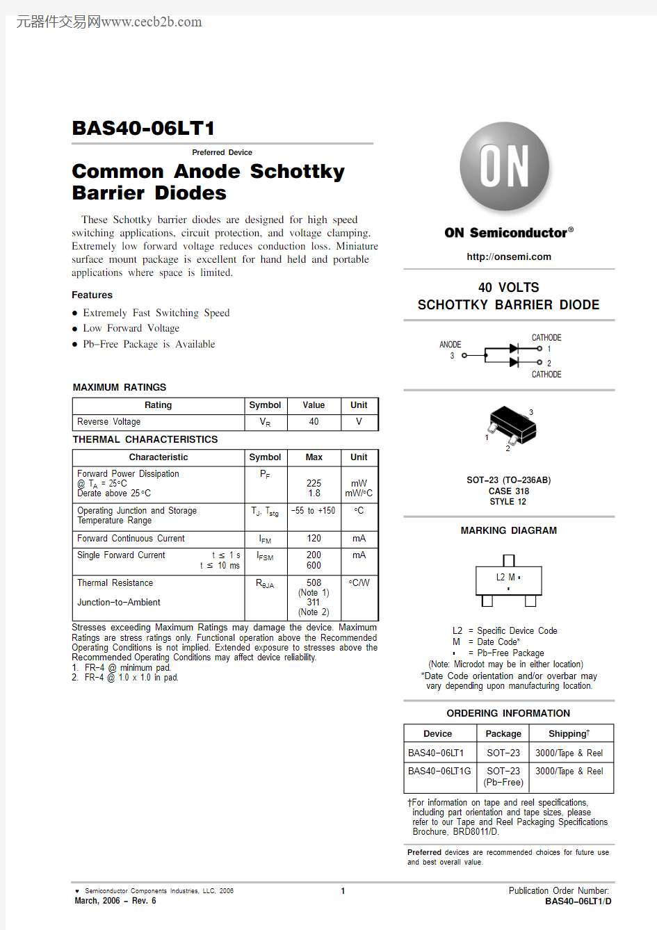
BAS40?06LT1
Preferred Device
Common Anode Schottky Barrier Diodes
These Schottky barrier diodes are designed for high speed switching applications, circuit protection, and voltage clamping. Extremely low forward voltage reduces conduction loss. Miniature surface mount package is excellent for hand held and portable applications where space is limited.
Features
?Extremely Fast Switching Speed
?Low Forward Voltage
?Pb?Free Package is Available
MAXIMUM RATINGS
Rating Symbol Value Unit Reverse Voltage V R40V THERMAL CHARACTERISTICS
Characteristic Symbol Max Unit
Forward Power Dissipation @ T A = 25°C
Derate above 25°C P F
225
1.8
mW
mW/°C
Operating Junction and Storage T emperature Range T J, T stg
?55 to +150°C
Forward Continuous Current I FM120mA
Single Forward Current t v 1 s
t v 10 ms I FSM200
600
mA
Thermal Resistance Junction?to?Ambient R q JA508
(Note 1)
311
(Note 2)
°C/W
Stresses exceeding Maximum Ratings may damage the device. Maximum
Ratings are stress ratings only. Functional operation above the Recommended
Operating Conditions is not implied. Extended exposure to stresses above the
Recommended Operating Conditions may affect device reliability.
1.FR?4 @ minimum pad.
2.FR?4 @ 1.0 x 1.0 in pad.
Preferred devices are recommended choices for future use
and best overall value.
https://www.wendangku.net/doc/081268817.html,
https://www.wendangku.net/doc/081268817.html,
2
ELECTRICAL CHARACTERISTICS (T A = 25°C unless otherwise noted)
Characteristic
Symbol Min Max Unit Reverse Breakdown Voltage
(I R = 10 m A)V (BR)R 40?V T otal Capacitance
(V R = 1.0 V, f = 1.0 MHz)C T ? 5.0pF Reverse Leakage
(V R = 25 V)I R ? 1.0m Adc Forward Voltage
(I F = 1.0 mAdc)V F ?380mVdc Forward Voltage
(I F = 10 mAdc)V F ?500mVdc Forward Voltage
(I F = 40 mAdc)
V F
?
1.0
Vdc
100
10
1.0
0.1
V R , REVERSE VOLTAGE (VOLTS)
I F , F O R W A R D C U R R E N T (m A )
Figure 3. Typical Capacitance
PACKAGE DIMENSIONS
SOT?23 (TO?236)CASE 318?08ISSUE AN
NOTES:
1.DIMENSIONING AND TOLERANCING PER ANSI Y14.5M, 198
2.
2.CONTROLLING DIMENSION: INCH.
3.MAXIMUM LEAD THICKNESS INCLUDES LEAD FINISH THICKNESS. MINIMUM LEAD THICKNESS IS THE MINIMUM THICKNESS OF BASE MATERIAL.
4.318?01 THRU ?07 AND ?09 OBSOLETE,NEW STANDARD 318?08.
SOLDERING FOOTPRINT*
VIEW C
DIM A MIN NOM MAX MIN MILLIMETERS
0.89 1.00 1.110.035INCHES
A10.010.060.100.001b 0.370.440.500.015c 0.090.130.180.003D 2.80 2.90 3.040.110E 1.20 1.30 1.400.047e 1.78 1.90 2.040.070L 0.100.200.300.0040.0400.0440.0020.0040.0180.0200.0050.0070.1140.1200.0510.0550.0750.0810.0080.012NOM MAX L1STYLE 12:
PIN 1.CATHODE
2.CATHODE
3.ANODE
2.10 2.40 2.64
0.0830.094
0.104
H E 0.350.540.690.0140.0210.029*For additional information on our Pb?Free strategy and soldering
details, please download the ON Semiconductor Soldering and Mounting T echniques Reference Manual, SOLDERRM/D.
ON Semiconductor and are registered trademarks of Semiconductor Components Industries, LLC (SCILLC). SCILLC reserves the right to make changes without further notice to any products herein. SCILLC makes no warranty, representation or guarantee regarding the suitability of its products for any particular purpose, nor does SCILLC assume any liability arising out of the application or use of any product or circuit, and specifically disclaims any and all liability, including without limitation special, consequential or incidental damages. “Typical” parameters which may be provided in SCILLC data sheets and/or specifications can and do vary in different applications and actual performance may vary over time. All operating parameters, including “Typicals” must be validated for each customer application by customer’s technical experts. SCILLC does not convey any license under its patent rights nor the rights of others. SCILLC products are not designed, intended, or authorized for use as components in systems intended for surgical implant into the body,or other applications intended to support or sustain life, or for any other application in which the failure of the SCILLC product could create a situation where personal injury or death may occur. Should Buyer purchase or use SCILLC products for any such unintended or unauthorized application, Buyer shall indemnify and hold SCILLC and its officers, employees,subsidiaries, affiliates, and distributors harmless against all claims, costs, damages, and expenses, and reasonable attorney fees arising out of, directly or indirectly, any claim of personal injury or death associated with such unintended or unauthorized use, even if such claim alleges that SCILLC was negligent regarding the design or manufacture of the part.SCILLC is an Equal Opportunity/Affirmative Action Employer. This literature is subject to all applicable copyright laws and is not for resale in any manner.
PUBLICATION ORDERING INFORMATION
- 家庭中的52个正面管教工具心得
- 34.引导孩子转移注意力
- 家庭中的52个正面管教工具第14章心得
- 家庭中的52个正面管教工具三观后感
- 家庭中的52个正面管教工具情绪管理读后感
- 正面管教的52个工具
- 材料力学试卷及答案
- 材料力学试卷及答案
- 《材料力学》期末考试试卷AB卷及答案
- 材料力学试卷及答案7套
- 材料力学(A)试卷
- 材料力学期末考试复习题及答案
- 材料力学期末试卷1(带答案)
- 材料力学期末考试试卷(含答案)
- 浙江大学城市学院《材料力学》样卷参考答案与评分标准题号1234567.docx
- 03-04浙大材料力学试卷
- 党旗飘扬我成长_小学作文_1
- 初二叙事作文:党旗飘扬我成长_1200字
- 在党旗下成长四年级作文
- 小学党旗引领我成长主题活动教案