MAX6407BS24+T中文资料
General Description
The MAX6406–MAX6411 is a family of ultra-low power circuits used for monitoring battery, power-supply, and regulated system voltages. Each detector contains a precision bandgap reference comparator and is trimmed to specified trip threshold voltages. These devices provide excellent circuit reliability and low cost by eliminating external components and adjustments when monitoring system voltages from 2.5V to 5.0V. A manual reset input is also included.
The MAX6406–MAX6411 assert a signal whenever the V CC supply voltage falls below a preset threshold.These devices are differentiated by their output logic configurations and preset threshold voltages. The MAX6406/MAX6409 (push-pull) and the MAX6408/MAX6411 (open-drain) have an active-low output (OUT is logic low when V CC is below V TH ). The MAX6407/MAX6410 have an active-high push-pull output (OUT is logic high when V CC is below V TH ). All parts are guaranteed to be in the correct output logic state for V CC down to 1V. The detector is designed to ignore fast transients on V CC . The MAX6406/MAX6407/MAX6408 have voltage thresholds between 2.20V and 3.08V in approximately 100mV increments. The MAX6409/MAX6410/MAX6411 have voltage thresholds between 3.30V and 4.63V in approximately 100mV increments.
Ultra-low supply current of 500nA (MAX6406/MAX6407/MAX6408) makes these parts ideal for use in portable equipment. These devices are available in 4-bump chip-scale packages (UCSP ).
Applications
Portable/Battery-Powered Equipment Cell Phones PDAs MP3 Players Pagers
Features
o Tiny 4-Bump (2 X 2) Chip-Scale Package, (Package Pending Full Qualification—Expected Completion Date 6/30/01. See UCSP Reliability Section for More Details.)o 70% Smaller Than SC70 Packages o Ultra-Low 500nA Supply Current (MAX6406/MAX6407/MAX6408)
o Factory-Trimmed Reset Thresholds from 2.20V to 4.63V in Approximately 100mV Increments o ±2.5% Threshold Accuracy (-40°C to +85°C)o Manual Reset Input
o Guaranteed OUT Valid to V CC = 1.0V
o Three Reset Output Logic Options: Active-Low Push-Pull, Active-High Push-Pull, and Active-Low Open-Drain o Immune to Short V CC Transients o No External Components
MAX6406–MAX6411
Voltage Detectors in 4-Bump (2 X 2)
Chip-Scale Package
Maxim Integrated Products 1
19-2041; Rev 1; 8/01
For pricing, delivery, and ordering information,please contact Maxim/Dallas Direct!at 1-888-629-4642, or visit Maxim’s website at https://www.wendangku.net/doc/067311822.html,.
The MAX6406–MAX6411 are available in factory-set V CC
detector thresholds from 2.20V to 4.63V, in approximately 0.1V increments. Choose the desired threshold suffix from Table 1and insert it in the blank space following “S”. There are 21standard versions with a required order increment of 2500pieces. Sample stock is generally held on the standard ver-sions only (Table1). Required order increment is 10,000 pieces for nonstandard versions (Table 2). Contact factory for avail-ability. All devices available in tape-and-reel only.
UCSP reliability is integrally linked to the user’s assembly
methods, circuit board material, and environment. Refer to the UCSP Reliability Notice in the UCSP Reliability section of this data sheet for more information.
Pin Configuration appears at end of data sheet.UCSP is a trademark of Maxim Integrated Products, Inc.
Ordering Information
Selector Guide
M A X 6406–M A X 6411
Voltage Detectors in 4-Bump (2 X 2) Chip-Scale Package
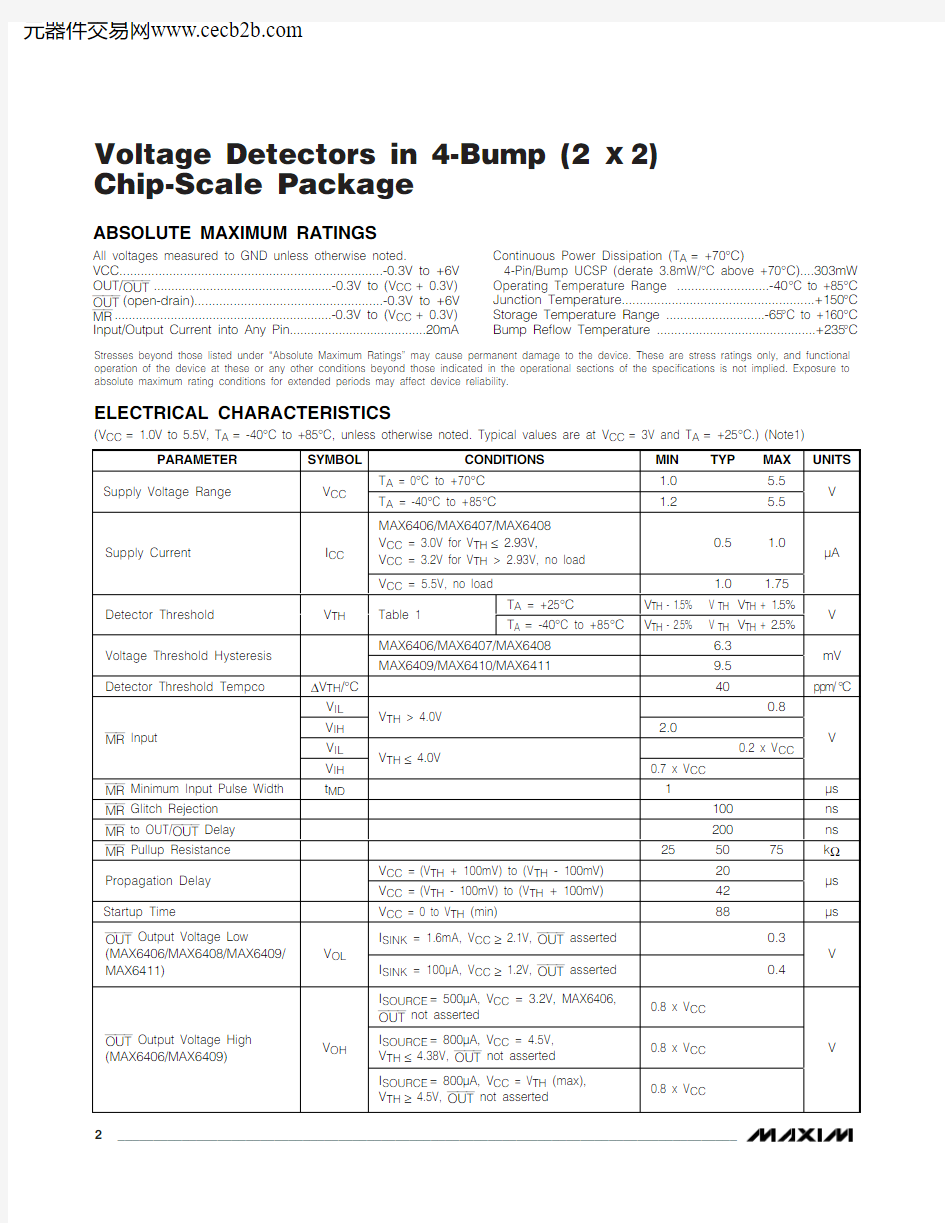
ABSOLUTE MAXIMUM RATINGS
Stresses beyond those listed under “Absolute Maximum Ratings” may cause permanent damage to the device. These are stress ratings only, and functional operation of the device at these or any other conditions beyond those indicated in the operational sections of the specifications is not implied. Exposure to absolute maximum rating conditions for extended periods may affect device reliability.
All voltages measured to GND unless otherwise noted.
VCC..........................................................................-0.3V to +6V OUT/OUT ...................................................-0.3V to (V CC + 0.3V)OUT (open-drain).....................................................-0.3V to +6V MR ..............................................................-0.3V to (V CC + 0.3V)Input/Output Current into Any Pin.......................................20mA
Continuous Power Dissipation (T A = +70°C)
4-Pin/Bump UCSP (derate 3.8mW/°C above +70°C)....303mW Operating Temperature Range ..........................-40°C to +85°C Junction Temperature......................................................+150°C Storage Temperature Range ............................-65°C to +160°C Bump Reflow Temperature .............................................+235°C
ELECTRICAL CHARACTERISTICS
(V CC = 1.0V to 5.5V, T A = -40°C to +85°C, unless otherwise noted. Typical values are at V CC = 3V and T A = +25°C.) (Note1)
MAX6406–MAX6411
Voltage Detectors in 4-Bump (2 X 2)
Chip-Scale Package
_______________________________________________________________________________________
3
Note 2:Guaranteed by design.
ELECTRICAL CHARACTERISTICS (continued)
(V CC = 1.0V to 5.5V, T A = -40°C to +85°C, unless otherwise noted. Typical values are at V CC = 3V and T A = +25°C.) (Note1)
Typical Operating Characteristics
(T A = +25°C, unless otherwise noted.)
00.30.20.10.50.40.90.80.70.61.0-40
-20
20
40
60
80
SUPPLY CURRENT vs. TEMPERATURE
TEMPERATURE (°C)S U P P L Y C U R R E N T (μA )
050
100
200
150
250
-40
-20
20
40
60
80
PROPAGATION DELAY (V CC FALLING)
vs. TEMPERATURE
TEMPERATURE (°C)
P R O P A G A T I O N D E L A Y (μs )
M A X 6406–M A X 6411
Voltage Detectors in 4-Bump (2 X 2) Chip-Scale Package 4_______________________________________________________________________________________
Typical Operating Characteristics (continued)
(T A = +25°C, unless otherwise noted.)
0402060
12010080140
-40
-20
20
40
60
80
PROPAGATION DELAY (V CC RISING)
vs. TEMPERATURE
TEMPERATURE (°C)P R O P A G A T I O N D E L A Y (μs )
01
1000
100
10
MAXIMUM TRANSIENT DURATION vs. THRESHOLD OVERDRIVE
500200
100
400300
THRESHOLD OVERDRIVE V TH - V CC (mV)
M A X I M U M T R A N S I E N T D U R A T I O N (μs )
MAX6406–MAX6411
Voltage Detectors in 4-Bump (2 X 2)
Chip-Scale Package
_______________________________________________________________________________________5
M A X 6406–M A X 6411
Detailed Description
Manual Reset Input
Many μP-based products require manual reset capabil-ity, allowing the operator, a test technician, or external logic circuit to initiate a reset. A logic low on MR asserts OUT/OUT . OUT/OUT remains asserted while MR is low.This input has an internal 50k ?pullup resistor, so it can be left open if it is not used. MR can be driven with TTL or CMOS logic levels, or with open-drain/collector out-puts. Connect a normally open momentary switch from MR to GND to create a manual reset function. If MR is driven from long cables or if the device is used in a noisy environment, connect a 0.1μF capacitor from MR to ground to provide additional noise immunity.
Applications Information
Interfacing to Different Logic
Voltage Components
The MAX6408/MAX6411 have an active-low, open-drain output. This output structure will sink current when OUT is asserted. Connect a pullup resistor from OUT to any supply voltage up to 5.5V (Figure 1). Select a resistor value large enough to allow a valid logic low (see Electrical Characteristics ), and small enough to register a logic high while supplying all input currents and leakage paths connected to the OUT line.
Voltage Detectors in 4-Bump (2 X 2) Chip-Scale Package 6
_______________________________________________________________________________________
Negative-Going V CC Transients
These devices are relatively immune to short-duration,negative-going V CC transients (glitches).
The Typical Operating Characteristics show the Maximum Transient Duration vs. Threshold Overdrive graph, for which output pulses are not generated. The graph shows the maximum pulse width that a negative-going V CC transient may typically have before the devices issue output signals. As the amplitude of the transient increases, the maximum allowable pulse width decreases.
UCSP Reliability
The chip-scale package (UCSP) represents a unique packaging form factor that may not perform equally to a packaged product through traditional mechanical reliabil-ity tests. CSP reliability is integrally linked to the user ’s assembly methods, circuit board material, and usage environment. The user should closely review these areas when considering use of a CSP package. Performance through Operating Life Test and Moisture Resistance remains uncompromised as it is primarily determined by the wafer-fabrication process.
Mechanical stress performance is a greater considera-tion for a CSP package. CSPs are attached through direct solder contact to the user ’s PC board, foregoing the inherent stress relief of a packaged product lead frame. Solder joint contact integrity must be https://www.wendangku.net/doc/067311822.html,rmation on Maxim ’s qualification plan, test data, and usage recommendations are detailed in the UCSP appli-cation note, which can be found on Maxim ’s website at https://www.wendangku.net/doc/067311822.html,.
Chip Information
TRANSISTOR COUNT: 512PROCESS: BiCMOS
MAX6406–MAX6411
Voltage Detectors in 4-Bump (2 X 2)
Chip-Scale Package
_______________________________________________________________________________________7
Figure 1. Interfacing to Different Logic Voltage Components
Pin Configuration
M A X 6406–M A X 6411
Voltage Detectors in 4-Bump (2 X 2) Chip-Scale Package Package Information
Maxim cannot assume responsibility for use of any circuitry other than circuitry entirely embodied in a Maxim product. No circuit patent licenses are implied. Maxim reserves the right to change the circuitry and specifications without notice at any time.
8_____________________Maxim Integrated Products, 120 San Gabriel Drive, Sunnyvale, CA 94086 408-737-7600?2001 Maxim Integrated Products
Printed USA
is a registered trademark of Maxim Integrated Products.