SY88982LMG TR;SY88982LMG;中文规格书,Datasheet资料

SY88982L
3.3V, 2.7Gbps High-Current, Low-Power
Laser Driver for FP/DFB Lasers
General Description
The SY88982L is a single 3.3V supply, low power
consumption, small form factor driver for
telecom/datacom applications using FP/DFB lasers
at data rates up to 2.7Gbps. The driver can deliver
modulation current up to 90mA, and the high
compliance voltage if offers, makes the part suitable
for high-current operation (with the laser AC- or DC-
coupled to it). This device is intended to be used
with Micrel’s MIC3003 Optical Transceiver
Management IC, which allows for both modulation
and bias current control and monitoring, automatic
power control, and temperature compensation.
All support documentation can be found on Micrel’s
web site at: https://www.wendangku.net/doc/1d2001731.html,.
Features
?2.4V minimum laser compliance voltage for high-
current DC-coupled applications
?48mA power supply current typical
?Operation up to 2.7Gbps
?Modulation current up to 90mA
?Designed for use with the MIC3003
?Laser may be DC- or AC-coupled
?Small form factor 16-pin (3mm x 3mm) QFN
package
Applications
?Multi-rate LAN, MAN applications up to 2.7Gbps:
FC, GbE, SONET OC3/12/24/48 and SDH
STM1/4/8/16
?SFF, SFP modules
Markets
?Telecom, Datacom
________________________________________________________________
Typical Application
Laser DC-Coupled to the Driver Laser AC-Coupled to the Driver
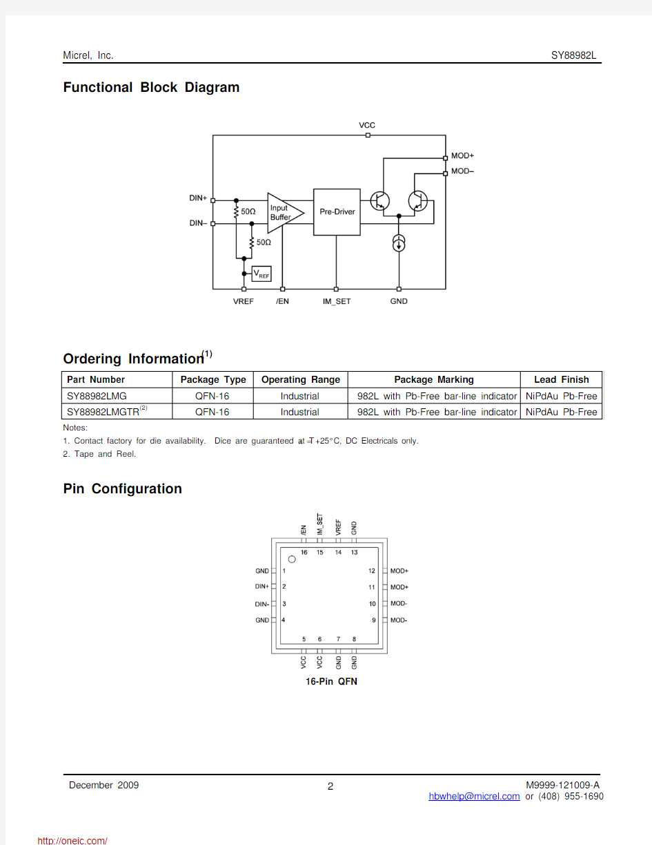
Functional Block Diagram
Ordering Information (1)
Notes:
1. Contact factory for die availability. Dice are guaranteed at T A = +25°C, DC Electricals only.
2. Tape and Reel.
Pin Configuration
16-Pin QFN
Pin Description
Truth Table
Notes:
1. I MOD = 0 when MOD+ = H.
2. Assuming that the laser is tied to MOD+.
December 2009 4
M9999-121009-A
hbwhelp@https://www.wendangku.net/doc/1d2001731.html, or (408) 955-1690
Absolute Maximum Ratings (1)
Supply Voltage (V IN ) ........................... –0.5V to +4.0V
CML Input Voltage (V IN )
.......... V CC –1.2V to V CC +0.5V TTL Control Input Voltage (V IN ) ...................
0V to V CC Lead Temperature (soldering, 20sec.) ........... +260°C
Storage Temperature (T s )
............... –65°C to +150°C Operating Ratings (2)
Supply Voltage (V CC )...........................+3.0V to +3.6V
Ambient Temperature (T A ) ................ –40°C to +85°C
Package Thermal Resistance (3)
QFN (θJA ) Still-air ............................................. 60°C/W (ψJB ) ......................................................... 33°C/W
DC Electrical Characteristics
T A = -40°C to 85°C and V CC = +3.0V to +3.6V, unless otherwise noted. Typical values are V CC = +3.3V, T A = 25°C,
I
= 60mA.
AC Electrical Characteristics
T A = -40°C to 85°C and V
CC = +3.0V to +3.6V, unless otherwise noted. Typical values are V CC = +3.3V, T A = 25°C, I = 60mA.
Notes:
1. Permanent device damage may occur if absolute maximum ratings are exceeded. This is a stress rating only and functional operation is
not implied at conditions other than those detailed in the operational sections of this data sheet. Exposure to absolute maximum ratings conditions for extended periods may affect device reliability. 2. The data sheet limits are not guaranteed if the device is operated beyond the operating ratings.
3. Package Thermal Resistance assumes exposed pad is soldered (or equivalent) to the devices most negative potential on the PCB. ψJB
uses a 4-layer and θJA in still air unless otherwise stated. 4. I CC = 48mA for worst-case conditions with I MOD = 90mA, T A = +85°C, V CC = 3.6. 5. Load = 15Ω.
6. Assuming VCC = 3.0V, Laser bandgap voltage = 1V, laser package inductance = 1nH, laser equivalent ser ies resistor = 5Ω, and damping
resistor = 10Ω.
December 2009 5
M9999-121009-A
hbwhelp@https://www.wendangku.net/doc/1d2001731.html, or (408) 955-1690
Typical Operating Characteristics
Test Circuit
Functional Characteristics
Input and Output Stages
Figure 1a. Simplified Input Stage
Figure 1b. Simplified Output Stage
Interfacing the Input to Different Logic Drivers
Figure 2a. DC-Coupling to LVPECL Driver
Figure 2b. AC-Coupling to LVPECL Driver
Figure 2c. AC-Coupling to CML Driver
Figure 2d. AC-Coupling to LVDS Driver
Application Information
The typical applications diagram on the first page shows how to connect the driver to the laser, single ended. To improve transition time and laser response, the laser can be driven differentially as shown in Figures 3 and 4. Driving the laser differentially will also minimize the crosstalk with the rest of the circuitry on the board, especially the receiver.
DC-Coupling
In addition to the low power consumption and high modulation current, the SY88982L offers a high compliance voltage. As can be seen in the “Typical Operating Characteristics” section (I MOD vs. V MOD curves), the minimum voltage needed at the output of the driver for proper operation is less than 600mV, leaving a large headroom, V CC-600mV, to the laser with the damping resistor. To show the importance of this high compliance voltage, consider the voltage drops along the path from V CC to ground through the laser, damping resistor, and driver:
V CC = Driver Headroom + V Rd + V laser
V Rd = Rd x I MOD
V laser = V band-gap + R laser x I MOD + Ldi/dt
V band-gap + R laser x I MOD = 1.6V at maximum for
a Fabry Perrot or a DFB laser.
Ldi/dt is the voltage drop due to the laser parasitic inductance during I MOD transitions. Assuming L = 1nH, t f = t f = 80ps (measured between 20% and 80% of I MOD), and I MOD = 70mA (42mA from 20% to 80%), then Ldi/dt will be equal to 525mV. This number can be minimized by making the laser leads as short as possible and using and RC compensation network between the cathode of the laser and ground or across the laser driver outputs as shown in Figure 3. To be able to drive the laser DC-coupled with a high current, it is necessary to keep the damping resistor as small as possible. For example, if the drop due to parasitic inductance of the laser is neglected (compensated for) and the maximum drop across the laser (1.6V) considered while keeping a minimum of 600mV headroom for the driver, then the maximum damping resistor that allows a 70mA modulation current into the laser is:
R dmax = (V CC-0.6V-1.6V)/0.07A
The worst case will be with V CC= 3.0V,
leading to R dmax = 11.4?
On the other hand, the small is the value of R d, the higher is the overshoot/undershoot on the optical signal from the laser. In the circuit shown in Figure 3, the RC compensation network across the driver outputs (MOD+ and MOD-) allows the user R d= 10?. The optical eye diagrams at data rates of 155Mbps/622Mbps/1.25Gbps/2.5Gbps, shown in “Functional Characteristics” section, are all obtained with the same circuit using R d = 10?, R Comp = 100?, and C Comp= 3pF. The compensation network may change from one board to another and from one type of laser to another. An additional compensation network (RC) can be added at the laser cathode for further compensation and eye smoothing.
Figure 3. Laser DC-Coupled
AC-Coupling
When trying to AC couple the laser to the driver, the headroom of the driver is no longer a problem since it is DC isolated from the laser with the coupling capacitor. At the output, the headroom of the driver is determined by the pull-up network. In Figure 4, the modulation current out of the driver is split between the pull-up network and the laser. If, for example, the total pull-up resistor is twice the sum of the damping resistor and laser equivalent series resistance, only two thirds (2/3) of the modulation current will be used by the laser. So, to keep most of the modulation current going through the laser, the total pull-up resistor must be kept as high as possible. One solution consists in using an inductor alone as pull-up, presenting a high impedance path for the modulation current and zero ohm (0?) path for the DC current offering a headroom of the driver equal to V CC and almost all the modulation current goes into the laser. The inductor alone will cause signal distortion, and, to improve that, a combination of resistors and inductors can be used (as shown on Figure 4). In this case, the headroom of the driver is V CC-R1 x αI MOD, where αI MOD is the portion of the modulation current that goes through the pull-up network.
When the laser is AC-coupled to the driver, the coupling capacitor creates a low-frequency cutoff in the circuit, and its value must be chosen as large as
slow down the fast signals edges, and, if its value is
too small, it won’t be able to hold a constant change
between the first bit and the last bit of a long string
of identical bits in a low data rate application. This
leads to higher pattern-dependent jitter in the
transmitter signal. 0.1μF is found to be good for all
applications from 155Mbps to 2.7Gbps.
AC-coupling the laser to the driver brings a solution
to the driver headroom problem at the expense of
extra components, loss of part of the modulation
current wasted in the pull-up network, and additional
power consumption.
Figure 4. Laser AC-Coupled
Package Information
16-Pin (3mm x 3mm) QFN
分销商库存信息:
MICREL
SY88982LMG TR SY88982LMG