JANTXV2N6790中文资料
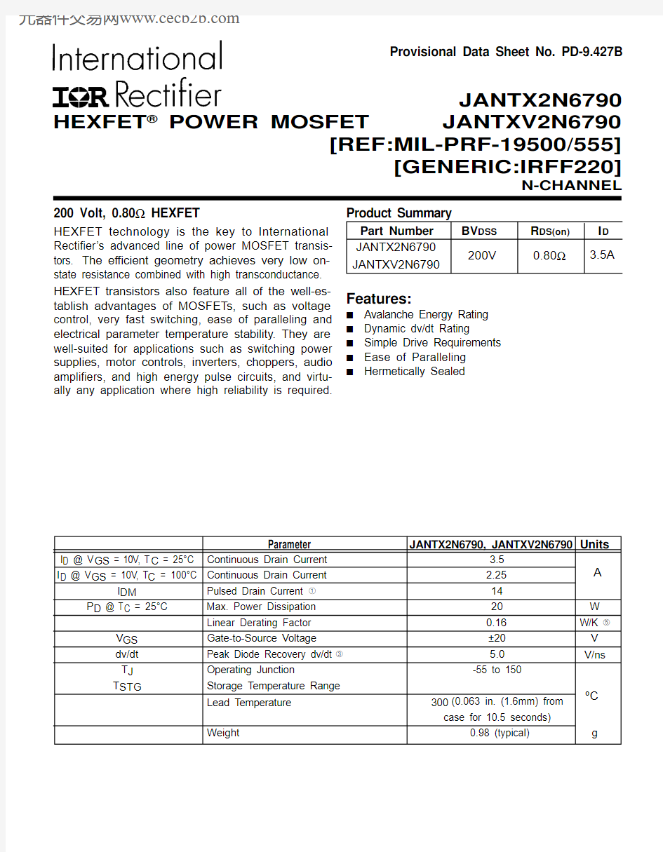
Product Summary
Part Number BV DSS R DS(on)I D JANTX2N6790JANTXV2N6790
Features:
s Avalanche Energy Rating s Dynamic dv/dt Rating
s Simple Drive Requirements s Ease of Paralleling s
Hermetically Sealed
N-CHANNEL
Provisional Data Sheet No. PD-9.427B
200 Volt, 0.80? HEXFET
HEXFET technology is the key to International Rectifier’s advanced line of power MOSFET transis-tors. The efficient geometry achieves very low on-state resistance combined with high transconductance.HEXFET transistors also feature all of the well-es-tablish advantages of MOSFETs, such as voltage control, very fast switching, ease of paralleling and electrical parameter temperature stability. They are well-suited for applications such as switching power supplies, motor controls, inverters, choppers, audio amplifiers, and high energy pulse circuits, and virtu-ally any application where high reliability is required.
JANTX2N6790
JANTXV2N6790
[REF:MIL-PRF-19500/555]
[GENERIC:IRFF220]
HEXFET ? POWER MOSFET Parameter
JANTX2N6790, JANTXV2N6790Units
I D @ V GS = 10V, T C = 25°C Continuous Drain Current 3.5I D @ V GS = 10V , T C = 100°C
Continuous Drain Current 2.25I DM
Pulsed Drain Current 14P D @ T C = 25°C
Max. Power Dissipation 20W Linear Derating Factor 0.16W/K V GS Gate-to-Source Voltage
±20V dv/dt Peak Diode Recovery dv/dt 5.0V/ns
T J Operating Junction
-55 to 150
T STG
Storage Temperature Range Lead Temperature 300
(0.063 in. (1.6mm) from case for 10.5 seconds)
Weight
0.98 (typical)
g
o
C
A
3.5A
0.80?
200V
元器件交易网https://www.wendangku.net/doc/1b7504693.html,
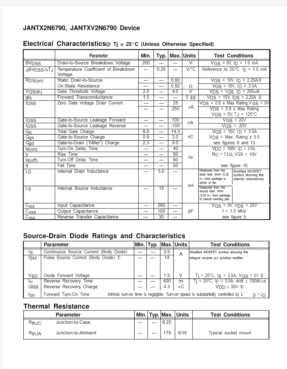
Thermal Resistance
Parameter
Min.Typ.Max.Units
Test Conditions
R thJC Junction-to-Case —— 6.25R thJA
Junction-to-Ambient
—
—
175
K/W
Typical socket mount
Source-Drain Diode Ratings and Characteristics
Parameter
Min.Typ.Max.Units
Test Conditions
I S Continuous Source Current (Body Diode)—— 3.5Modified MOSFET symbol showing the I SM
Pulse Source Current (Body Diode)
—
—
14
integral reverse p-n junction rectifier.
V SD Diode Forward Voltage —— 1.5V T j = 25°C, I S = 3.5A, V GS = 0V t rr Reverse Recovery Time ——400ns T j = 25°C, I F = 3.5A, di/dt ≤ 100A/μs
Q RR Reverse Recovery Charge —— 4.3μC
V DD ≤ 50V
t on
Forward Turn-On Time
Intrinsic turn-on time is negligible. Turn-on speed is substantially controlled by L S + L D .
Electrical Characteristics @ Tj = 25°C (Unless Otherwise Specified)
DS = 25V
f = 1.0 MHz see figure 5
A
Fig. 1 — T ypical Output Characteristics
T C = 25°C Fig. 2 — T ypical Output Characteristics
T C = 150°C
Fig. 3 — Typical Transfer Characteristics Fig. 4 — Normalized On-Resistance Vs.Temperature
Fig. 5 — T ypical Capacitance Vs. Drain-to-Source
Voltage Fig. 6 — T ypical Gate Charge Vs. Gate-to-Source
Voltage
Fig. 10b — Switching Time Waveforms
Fig. 10a — Switching Time Test Circuit Fig. 8 — Maximum Safe Operating Area
Fig. 9 — Maximum Drain Current Vs. Case Temperature
Fig. 7 — Typical Source-to-Drain Diode Forward
Voltage
Fig. 13a — Gate Charge T est Circuit
Fig. 12a — Unclamped Inductive T est Circuit Fig. 12b — Unclamped Inductive Waveforms
Fig. 11 — Maximum Effective Transient Thermal Impedance, Junction-to-Case Vs. Pulse Duration
JANTX2N6790, JANTXV2N6790 Device
Repetitive Rating; Pulse width limited by maximum junction temperature.(see figure 11)
@ V DD = 50V , Starting T J = 25°C,
E AS = [0.5 * L * (I L 2) * [BV DSS /(BV DSS -V DD )]Peak I L = 3.5A, V GS = 10V , 25 ≤ R G ≤ 200?
WORLD HEADQUARTERS: 233 Kansas St., El Segundo, California 90245, Tel: (310) 322 3331EUROPEAN HEADQUARTERS: Hurst Green, Oxted, Surrey RH8 9BB, UK Tel: ++ 44 1883 732020IR CANADA: 7321 Victoria Park Ave., Suite 201, Markham, Ontario L3R 2Z8, Tel: (905) 475 1897
IR GERMANY: Saalburgstrasse 157, 61350 Bad Homburg Tel: ++ 49 6172 96590
IR ITALY: Via Liguria 49, 10071 Borgaro, Torino Tel: ++ 39 11 451 0111
IR FAR EAST: K&H Bldg., 2F, 3-30-4 Nishi-Ikeburo 3-Chome, Toshima-Ki, Tokyo Japan 171 Tel: 81 3 3983 0086
IR SOUTHEAST ASIA: 315 Outram Road, #10-02 Tan Boon Liat Building, Singapore 0316 Tel: 65 221 8371
https://www.wendangku.net/doc/1b7504693.html,/Data and specifications subject to change without notice.
10/96
All dimensions are shown millimeters (inches)