W55F05中文资料

W55FXX
SERIAL FLASH EEPROM SERIES
Publication Release Date: August 1996
GENERAL DESCRIPTION
The W55FXX is a serial input/output flash EEPROM series that is typically used as the memory cell
of a W51300 (voice recorder controller) or the ROM code emulator for the PowerSpeech TM
series.The single voltage supply eliminates the need for an extra pump circuit during programming and erasing.
FEATURES
?Provides CLK, ADDR, and DATA pins to operate with Winbond PowerSpeech TM series ?512K/1M/2M memory sizes available ?Directly cascadable for longer duration ?
Fast frame-write operation
?Frame (32 bits) program cycle time: 400 μS (typ.)?Fast whole-chip-erase duration: 50 mS (max.)?Read data access time: 500 nS (max.)?Program/erase cycles: 10,000 (typ.)?Data retention: 10 years (typ.)?
Low power consumption:?Operating: 5 mA (typ.)?Standby: 2 μA (typ.)
PIN CONFIGURATION
W55FXX
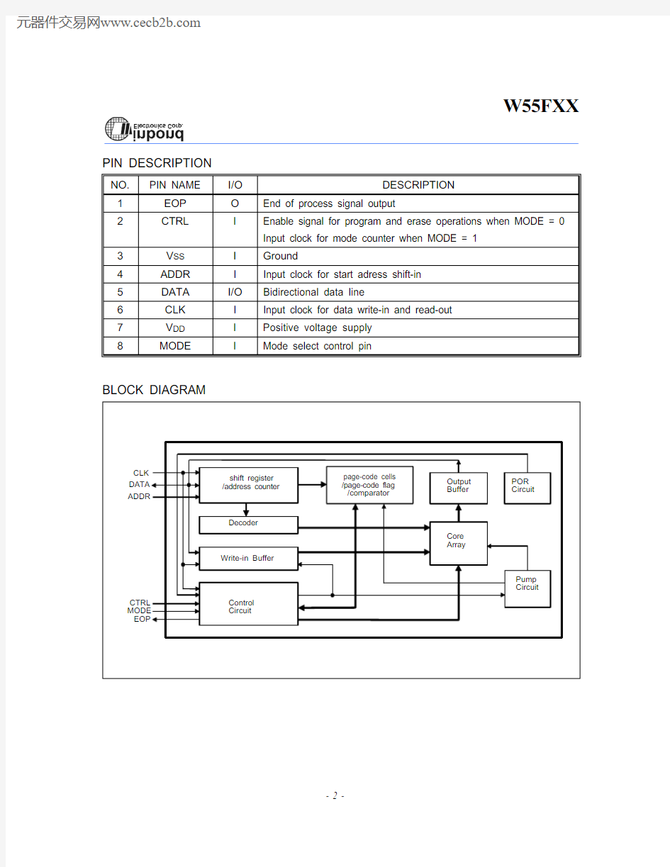
PIN DESCRIPTION
NO.PIN NAME I/O DESCRIPTION
1EOP O End of process signal output
2CTRL I Enable signal for program and erase operations when MODE = 0Input clock for mode counter when MODE = 13V SS I Ground
4ADDR I Input clock for start adress shift-in 5DATA I/O
Bidirectional data line
6CLK I Input clock for data write-in and read-out 7V DD I Positive voltage supply 8
MODE
I
Mode select control pin
BLOCK DIAGRAM
W55FXX
Publication Release Date: August 1996
ABSOLUTE MAXIMUM RATINGS
PARAMETER
SYMBOL CONDITION
RATED VALUE
UNIT Operating Temp.T OPR -0 to +70°C Storage Temp.T STG --65 to +150°C Power Supply V DD ?V SS --0.3 to +7.0V Input DC Voltage
V DC All pins -0.5 to V DD +1.0V Transient Voltage (< 20 nS)
V TRAN
All pins
-1.0 to V DD +1.0
V
Note: Exposure to conditions beyond those listed under Absolute Maximum Ratings may adversely affect the life and reliability of the device.
DC CHARACTERISTICS
(V DD = 4.5V, V SS = 0V, T A = 25° C)
PARAMETER SYMBOL CONDITIONS
LIMITS UNIT MIN.
TYP.MAX.Operating voltage V DD - 2.4
(Note)
4.5
5.5V Standby current I SB All inputs = GND DATA & EOP open -
24μA Operating current
I OP
In read mode DATA & EOP open F OSC = 1 MHz
-5
10
mA
Input voltage High V IH All input pins 2.0V DD V Low V IL -0.3-0.8V Output current
Sink I OL V OL = 0.5V 2.55-mA Drive
I OH V OH = 4.0V -2.5-5-mA Input leakage current of CTRL, MODE I LI1V IN = 4.5V -- 4.5μA Input leakage current of DATA
I LI2
V IN = 0V
--
-4.5
μA
Note: For been working with W52900, the minimum operating voltage couldn't be less than 3.6 volt.
W55FXX
AC CHARACTERISTICS
(V DD = 4.5V, V SS = 0V, T A = 25° C)
PARAMETER
SYMBOL CONDITIONS
MIN.TYP.MAX.UNIT MODE pulse width T MP -1--μS CTRL pulse width T WP Page coding mode
400-700μS Clock frequency of ADDR F ADDR ---1MHz Clock frequency of CLK F CLK ---1MHz Clock frequency of CTRL F CTRL ---1MHz Interval between ADDR end & CLK begin
T I Read/Write mode 1--μS Interval between CLK &CTRL
T GCC Write mode 1--μS Interval between ADDR &CTRL
T GCA Page coding mode 1--μS Interval between addressing end & block-erase begin T AE Block erase mode 1--μS Interval between MODE rising edge & CTRL clock begin
T MB
Mode selection
500
-
-
nS
Interval between CTRL clock end & MODE falling edge T ME Mode selection
500--nS Interval between MODE falling edge & another pin active
T GM
-
1
-
-
μS
Data access time T RA Read mode --500nS Data set up time T WS Write mode
250--nS T AS -250--nS Data hold time
T RH Read mode 0--nS T WH Write mode
10--nS T AH
-10--nS Programming duration T PR Write mode 400--μS Whole-chip-erase time T WE Whole-chip-erase mode
45-50mS Block-erase time
T BE
Block-erase mode
40
-
45
mS
W55FXX
Publication Release Date: August 1996
TIMING WAVEFORM
W55FXX
APPLICATION CIRCUITS (for reference only)
ORDERING INFORMATION
PART NO.MEMORY SIZE
W55F05512K BITS W55F101M BITS W55F20
2M BITS
W55FXX
Publication Release Date: August 1996
Headquarters
No. 4, Creation Rd. III,
Science-Based Industrial Park,Hsinchu, Taiwan TEL: 886-3-5770066FAX: 886-3-5792697
https://www.wendangku.net/doc/1e12919611.html,/
Voice & Fax-on-demand: 886-2-7197006
Taipei Office
11F, No. 115, Sec. 3, Min-Sheng East Rd.,Taipei, Taiwan
TEL: 886-2-7190505FAX: 886-2-7197502
Winbond Electronics (H.K.) Ltd.
Rm. 803, World Trade Square, Tower II,123 Hoi Bun Rd., Kwun Tong,Kowloon, Hong Kong TEL: 852-********FAX: 852-********
Winbond Electronics North America Corp.Winbond Memory Lab.
Winbond Microelectronics Corp.Winbond Systems Lab.
2730 Orchard Parkway, San Jose,CA 95134, U.S.A.TEL: 1-408-9436666FAX: 1-408-9436668
Note: All data and specifications are subject to change without notice.