RU6888R
RU6888
N-Channel Advanced Power MOSFET
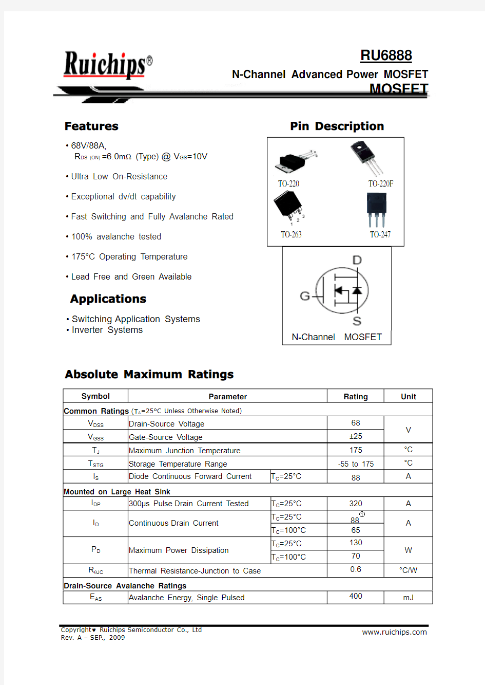
MOSFET Features Pin Description
Applications
Symbol Parameter Rating Unit Common Ratings(T A=25°C Unless Otherwise Noted)
V DSS Drain-Source Voltage68
V GSS Gate-Source Voltage±25
V T J Maximum Junction Temperature175°C
T STG Storage Temperature Range-55 to 175°C
I S Diode Continuous Forward Current T C=25°C88A Mounted on Large Heat Sink
I DP300μs Pulse Drain Current Tested T
C
=25°C320A
T C=25°C88①
I D Continuous Drain Current
T C=100°C65
A
T C=25°C130
P D Maximum Power Dissipation
T C=100°C70
W RθJC Thermal Resistance-Junction to Case0.6°C/W Drain-Source Avalanche Ratings
E AS Avalanche Energy, Single Pulsed400mJ ?68V/88A,
R DS (ON)=6.0m? (Type)@V GS=10V
?Ultra Low On-Resistance
?Exceptional dv/dt capability
?Fast Switching and Fully Avalanche Rated
?100% avalanche tested
?175°C Operating Temperature
?Lead Free and Green Available
?Switching Application Systems
?Inverter Systems
Absolute Maximum Ratings
TO-220 TO-220F
TO-263 TO-247
N-Channel MOSFET
Electrical Characteristics
(T A =25°C Unless Otherwise Noted)
RU6888Symbol
Parameter Test Condition Min.
Typ.
Max.
Unit
Static Characteristics BV DSS Drain-Source Breakdown Voltage V GS =0V, I DS =-250μA 68
V V DS =68V, V GS =0V
1I DSS Zero Gate Voltage Drain Current T J =85°C
30
μA V GS(th)Gate Threshold Voltage V DS =V GS , I DS =-250μA 2
34V I GSS Gate Leakage Current
V GS =±25V, V DS =0V ±100nA R DS(ON)
②
Drain-Source On-state Resistance
V GS = 10V, I DS =35A
6
8
m ?
Notes:
①Current limited by wire bond.
②Pulse test ;Pulse width ≤300μs, duty cycle ≤2%.
③Guaranteed by design, not subject to production testing.
Diode Characteristics V SD
②
Diode Forward Voltage I SD =20A, V GS =0V 0.84V t rr Reverse Recovery Time 49ns Q rr
Reverse Recovery Charge
I SD =40A, dl SD /dt=100A/μs
93
nC Dynamic Characteristics
③
R G Gate Resistance
V GS =0V,V DS =0V,F=1MHz 1.4?C iss Input Capacitance 2900C oss Output Capacitance
340C rss Reverse Transfer Capacitance V GS =0V,
V DS = 30V,
Frequency=1.0MHz
200pF
t d(ON)Turn-on Delay Time 13t r Turn-on Rise Time 15t d(OFF)Turn-off Delay Time 29t f
Turn-off Fall Time
V DD =30V, R L =30?,I DS =1A, V GEN =10V,R G =8?
55
ns
Gate Charge Characteristics
③
Q g Total Gate Charge 65Q gs Gate-Source Charge 12Q gd
Gate-Drain Charge
V DS =30V, V GS =10V,I DS =40A
21
nC
Typical Characteristics
Power Dissipation
Drain Current
P t o t -P o w e r (W )
I D - D r a i n C u r r e n t (A )
T j - Junction Temperature (°C)
T j - Junction Temperature (°C)
Safe Operation Area
Thermal Transient Impedance
I D - D r a i n C u r r e n t (A )
N o r m a l i z e d E f f e c t i v e T r a n s i e n t
V DS - Drain-Source Voltage (V)
Square Wave Pulse Duration (sec)
Typical Characteristics
Output Characteristics
Drain-Source On Resistance
I D - D r a i n C u r r e n t (A )
R D S (O N )- O n R e s i s t a n c e (m Ω)
V DS - Drain-Source Voltage (V)
I D -Drain Current (A)
Drain-Source On Resistance Gate Threshold Voltage
R D S (O N )- O n - R e s i s t a n c e (m )
N o r m a l i z e d T h r e s h o l d V o l t a g e
V GS -Gate-Source Voltage (V)
T j - Junction Temperature (°C)
Typical Characteristics
Drain-Source On Resistance
Source-Drain Diode Forward
N o r m a l i z e d O n R e s i s t a n c e
I S - S o u r c e C u r r e n t (A )
T j - Junction Temperature (°C)
V SD - Source-Drain Voltage (V)
Capacitance
Gate Charge
C - C a p a c i t a n c e (p F )
V G S - G a t e -S o u r c e V o l t a g e (V )
V DS - Drain-Source Voltage (V)
Q G - Gate Charge (nC)
Avalanche Test Circuit and Waveforms
Switching Time Test Circuit and Waveforms
Ordering and Marking Information
RU6888
Package (Available)
R : TO-220; S: TO-263 ; P: TO-220F; Q: TO-247
Operating Temperature Range
C :-55 to 175 oC
Assembly Material
G : Green & Lead Free
Packaging
T : TUBE
TR : Tape & Reel
Package Information
TO-220FB-3L
ALL DIMENSIONS REFER TO JEDEC STANDARD DO NOT INCLUDE MOLD FLASH OR PROTRUSIONS
MM
INCH MM
INCH SYMBOL
MIN NOM MAX MIN NOM MAX SYMBOL MIN NOM MAX MIN NOM MAX A 4.40 4.57 4.700.1730.1800.185?p1 1.40
1.50 1.60
0.055
0.0590.063
A1 1.27 1.30 1.330.0500.0510.052e 2.54BSC 0.1BSC A2 2.35 2.40 2.500.0930.0940.098e1 5.08BSC 0.2BSC b 0.77-0.900.030-0.035H1 6.40 6.50 6.600.2520.2560.260b2 1.23- 1.360.048-0.054L 12.75-13.170.502-0.519C 0.480.500.520.0190.0200.021L1-- 3.95
--0.156D 15.4015.6015.800.6060.6140.622L2 2.50REF.0.098REF.D19.009.109.200.3540.3580.362?p 3.57 3.60 3.630.1410.1420.143DEP 0.050.100.200.0020.0040.008Q
2.73 2.80 2.870.1070.1100.113E 9.709.9010.100.3820.3890.398θ15°7°9°5°7°9°E1-8.70--0.343-θ2
1°
3°
5°
1°
3°
5°E2
9.80
10.00
10.20
0.386
0.394
0.401
TO-263-2L
ALL DIMENSIONS REFER TO JEDEC STANDARD DO NOT INCLUDE MOLD FLASH OR PROTRUSIONS
MM
INCH MM
INCH SYMBOL
MIN NOM MAX MIN NOM MAX SYMBOL
MIN NOM MAX MIN NOM MAX A 4.40 4.57 4.700.1730.1800.185L 2.00 2.30 2.600.0790.0900.102A100.100.2500.0040.010L3 1.17 1.27 1.400.0460.0500.055A2 2.59 2.69 2.790.1020.1060.110L1-- 1.70
-
-0.067
b 0.77-0.900.030-0.035L40.25BSC 0.01BSC b1 1.23- 1.360.048-0.052L2
2.50REF.0.098REF.
c 0.34-0.470.013-0.019θ0°-8°0°-8°C1 1.22- 1.320.048-0.052θ15°7°9°5°7°9°D 8.608.708.800.3380.3430.346θ2
1°3°5°1°3°5°E 10.0010.1610.26
0.394
0.40.404
DEP 0.050.100.200.0020.0040.008e 2.54BSC 0.1BSC ?p1
1.40
1.50
1.60
0.055
0.059
0.063H
14.70
15.10
15.50
0.579
0.594
0.610
TO-220F-3L
ALL DIMENSIONS REFER TO JEDEC STANDARD DO NOT INCLUDE MOLD FLASH OR PROTRUSIONS
MM
INCH MM
INCH SYMBOL
MIN NOM MAX MIN NOM MAX SYMBOL MIN NOM MAX MIN NOM MAX E 9.9610.1610.360.3920.4000.408?p3
- 3.450--0.136-A 4.50 4.70 4.900.1770.1850.193θ15°7°9°5°7°9°A1 2.34 2.54 2.740.0920.1000.108θ2
-45°--45°-A20.95 1.05 1.150.0370.0410.045DEP 0.050.100.150.0020.0040.006A30.420.520.620.0170.0200.024F1 1.90 2.00 2.100.0750.0790.083A4 2.65 2.75 2.850.1040.1080.112F213.6113.8114.010.5360.5440.552c -0.50--0.020-F3 3.20 3.30 3.400.1260.1300.134D 15.6715.8716.070.6170.6250.633G 3.25 3.45 3.650.1280.1360.144Q 8.809.009.200.3460.3540.362G1 5.90 6.00 6.100.2320.2360.240H1 6.48 6.68 6.88
0.255
0.2630.271
G2 6.907.007.100.2720.2760.280e 2.54BSC 0.1BSC b1 1.17 1.20 1.240.0460.0470.048?p - 3.183--0.125-b20.770.80.850.0300.0310.033L 12.7812.9813.180.5030.5110.519b3 1.10 1.30 1.500.0430.0510.059D18.999.199.390.3540.3620.370E19.810.0010.200.3860.3940.412?p1 1.40 1.50 1.600.0550.0590.063K1
0.75
0.8
0.85
0.030
0.031
0.033
?p2
1.15
1.20
1.25
0.045
0.047
0.049
TO-247
ALL DIMENSIONS REFER TO JEDEC STANDARD DO NOT INCLUDE MOLD FLASH OR PROTRUSIONS
MM INCH
MM INCH SYMBOL
MIN MAX MIN
MAX SYMBOL
MIN MAX MIN MAX A 4.850 5.1500,1910.200E2 3.600 REF
0.142 REF
A1 2.200 2.6000.0870.102L 40.90041.300 1.610 1.626B 1.000 1.4000.0390.055L124.80025.1000.9760.988b1 2.800 3.2000.1100.126L220.30020.6000.7990.811b2 1.800 2.2000.0710.087Φ7.100
7.300
0.280
0.287
c 0.5000.7000.0200.028e 5.450 TYP 0.215 TYP c1 1.900 2.1000.0750.083H 5.980 REF.0.235 REF.D 15.450
15.750
0.608
0.620
h
0.000
0.300
0.000
0.012
E1
3.500 REF.0.138 REF.
Customer Service
Worldwide Sales and Service:
Sales@https://www.wendangku.net/doc/217081779.html,
Technical Support:
Technical@https://www.wendangku.net/doc/217081779.html,
Investor Relations Contacts:
Investor@https://www.wendangku.net/doc/217081779.html,
Marcom Contact:
Marcom@https://www.wendangku.net/doc/217081779.html,
Editorial Contact:
Editorial@https://www.wendangku.net/doc/217081779.html,
HR Contact:
HR@https://www.wendangku.net/doc/217081779.html,
Legal Contact:
Legal@https://www.wendangku.net/doc/217081779.html,
Shen Zhen RUICHIPS Semiconductor CO., LTD
Room501,the5floor An Tong Industrial Building,
NO.207Mei Hua Road Fu Tian Area Shen Zhen City,CHINA TEL:(86-755) 8311-5334
FAX: (86-755) 8311-4278
E-mail: Sales-SZ@https://www.wendangku.net/doc/217081779.html,