74HC27

TL F 5300MM54HC27 MM74HC27 Triple 3-Input NOR Gate
January1988 MM54HC27 MM74HC27
Triple3-Input NOR Gate
General Description
These NOR gates utilize advanced silicon-gate CMOS tech-
nology to achieve operating speeds similar to LS-TTL gates
with the low power consumption of standard CMOS inte-
grated circuits All gates have buffered outputs providing
high noise immunity and the ability to drive10LS-TTL loads
The54HC 74HC logic family is functionally as well as pin-
out compatible with the standard54LS 74LS logic family
All inputs are protected from damage due to static dis-
charge by internal diode clamps to V CC and ground
Features
Y Typical propagation delay 8ns
Y Wide operating supply voltage range 2–6V
Y Low input current k1m A
Y Low quiescent supply current 20m A maximum
(74HC Series)
Y Fanout of10LS-TTL Loads
Connection and Logic Diagrams
Dual-In-Line Package
TL F 5300–1
Top View
Order Number MM54HC27or MM74HC27
TL F 5300–2
C1995National Semiconductor Corporation RRD-B30M105 Printed in U S A
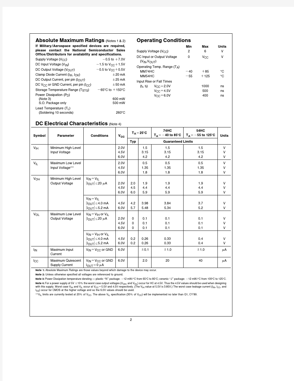
Absolute Maximum Ratings(Notes1 2) If Military Aerospace specified devices are required please contact the National Semiconductor Sales Office Distributors for availability and specifications Supply Voltage(V CC)b0 5to a7 0V DC Input Voltage(V IN)b1 5to V CC a1 5V DC Output Voltage(V OUT)b0 5to V CC a0 5V Clamp Diode Current(I IK I OK)g20mA DC Output Current per pin(I OUT)g25mA DC V CC or GND Current per pin(I CC)g50mA Storage Temperature Range(T STG)b65 C to a150 C Power Dissipation(P D)
(Note3)600mW S O Package only500mW Lead Temperature(T L)
(Soldering10seconds)260 C Operating Conditions
Min Max Units Supply Voltage(V CC)26V DC Input or Output Voltage0V CC V (V IN V OUT)
Operating Temp Range(T A)
MM74HC b40a85 C MM54HC b55a125 C Input Rise or Fall Times
V CC e2 0V
(t r t f)1000ns V CC e4 5V500ns
V CC e6 0V400ns
DC Electrical Characteristics(Note4)
T A e25 C 74HC54HC
Symbol Parameter Conditions V CC T A eb40to85 C T A eb55to125 C Units
Typ Guaranteed Limits
V IH Minimum High Level2 0V1 51 51 5V Input Voltage4 5V3 153 153 15V
6 0V4 24 24 2V
V IL Maximum Low Level2 0V0 50 50 5V Input Voltage 4 5V1 351 351 35V
6 0V1 81 81 8V
V OH Minimum High Level V IN e V IL
Output Voltage l I OUT l s20m A2 0V2 01 91 91 9V
4 5V4 54 44 44 4V
6 0V6 05 95 95 9V
V IN e V IL
l I OUT l s4 0mA4 5V4 23 983 843 7V
l I OUT l s5 2mA6 0V5 75 485 345 2V V OL Maximum Low Level V IN e V IH or V IL
Output Voltage l I OUT l s20m A2 0V00 10 10 1V
4 5V00 10 10 1V
6 0V00 10 10 1V
V IN e V IH or V IL
l I OUT l s4 0mA4 5V0 20 260 330 4V
l I OUT l s5 2mA6 0V0 20 260 330 4V I IN Maximum Input V IN e V CC or GND6 0V g0 1g1 0g1 0m A
Current
I CC Maximum Quiescent V IN e V CC or GND6 0V2 02040m A
Supply Current I OUT e0m A
Note1 Absolute Maximum Ratings are those values beyond which damage to the device may occur
Note2 Unless otherwise specified all voltages are referenced to ground
Note3 Power Dissipation temperature derating plastic‘‘N’’package b12mW C from65 C to85 C ceramic‘‘J’’package b12mW C from100 C to125 C Note4 For a power supply of5V g10%the worst case output voltages(V OH and V OL)occur for HC at4 5V Thus the4 5V values should be used when designing with this supply Worst case V IH and V IL occur at V CC e5 5V and4 5V respectively (The V IH value at5 5V is3 85V )The worst case leakage current(I IN I CC and I OZ)occur for CMOS at the higher voltage and so the6 0V values should be used
V IL limits are currently tested at20%of V CC The above V IL specification(30%of V CC)will be implemented no later than Q1 CY’89
2
AC Electrical Characteristics V CC e5V T A e25 C C L e15pF t r e t f e6ns
Symbol Parameter Conditions Typ Guaranteed
Units Limit
t PHL t PLH Maximum Propagation815ns
Delay
AC Electrical Characteristics V CC e2 0V to6 0V C L e50pF t r e t f e6ns(unless otherwise specified)
T A e25 C 74HC54HC
Symbol Parameter Conditions V CC T A eb40to85 C T A eb55to125 C Units
Typ Guaranteed Limits
t PHL t PLH Maximum Propagation2 0V4590113134ns Delay4 5V9182327ns
6 0V8151923ns
t TLH t THL Maximum Output Rise2 0V307595110ns and Fall Time4 5V8151922ns
6 0V7131619ns
C P
D Power Dissipation(per gate)36pF
Capacitance(Note5)
C IN Maximum Input5101010pF
Capacitance
Note5 C PD determines the no load dynamic power consumption P D e C PD V CC2f a I CC V CC and the no load dynamic current consumption I S e C PD V CC f a I CC Physical Dimensions inches(millimeters)
Order Number MM54HC27J or MM74HC27J
NS Package Number J14A
3
M M 54H C 27 M M 74H C 27T r i p l e 3-I n p u t N O R G a t e
Physical Dimensions inches (millimeters)(Continued)
Order Number MM74HC27N NS Package Number N14A
LIFE SUPPORT POLICY
NATIONAL’S PRODUCTS ARE NOT AUTHORIZED FOR USE AS CRITICAL COMPONENTS IN LIFE SUPPORT DEVICES OR SYSTEMS WITHOUT THE EXPRESS WRITTEN APPROVAL OF THE PRESIDENT OF NATIONAL SEMICONDUCTOR CORPORATION As used herein 1 Life support devices or systems are devices or 2 A critical component is any component of a life systems which (a)are intended for surgical implant support device or system whose failure to perform can into the body or (b)support or sustain life and whose be reasonably expected to cause the failure of the life failure to perform when properly used in accordance support device or system or to affect its safety or with instructions for use provided in the labeling can effectiveness
be reasonably expected to result in a significant injury to the user
National Semiconductor National Semiconductor National Semiconductor National Semiconductor Corporation
Europe
Hong Kong Ltd
Japan Ltd
1111West Bardin Road
Fax (a 49)0-180-5308586
13th Floor Straight Block Tel 81-043-299-2309