关于51单片机英文文献的英文翻译

利用单片机的定时器
6.1 前言
这一章包含一个描述的定时器系统微控制器,包括通用定时器,该定时器,和看门狗。
6.2 总体结构和功能,计时器系统
时间是必不可少的操作微控制器系统,可以生成信号的精确确定的期限,或外部事件计数。这原因,定时器子系统,是目前所有的微控制器的实现,和涵盖的范围广泛的功能包括:
?生成精确的时间间隔
?测量时间的外部事件
?计数外部事件。
多数微控制器提供专用定时器,或使用通用计时器实现以下功能:
?实时时钟
?产生的脉冲宽度调制(脉宽调制)信号
?看门狗检测程序失控情况。
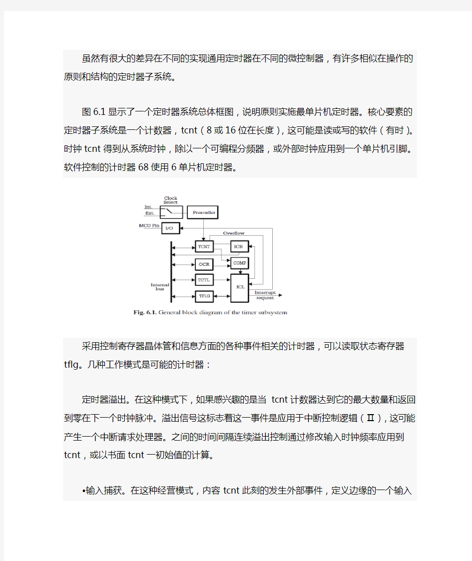
虽然有很大的差异在不同的实现通用定时器在不同的微控制器,有许多相似在操作的原则和结构的定时器子系统。
图6.1显示了一个定时器系统总体框图,说明原则实施最单片机定时器。核心要素的定时器子系统是一个计数器,tcnt(8或16位在长度),这可能是读或写的软件(有时)。时钟tcnt 得到从系统时钟,除以一个可编程分频器,或外部时钟应用到一个单片机引脚。软件控制的计时器68使用6单片机定时器。
采用控制寄存器晶体管和信息方面的各种事件相关的计时器,可以读取状态寄存器tflg。几种工作模式是可能的计时器:
定时器溢出。在这种模式下,如果感兴趣的是当tcnt计数器达到它的最大数量和返回到零在下一个时钟脉冲。溢出信号这标志着这一事件是应用于中断控制逻辑(Ⅱ),这可能产生一个中断请求处理器。之间的时间间隔连续溢出控制通过修改输入时钟频率应用到tcnt,或以书面tcnt 一初始值的计算。
?输入捕获。在这种经营模式,内容tcnt此刻的发生外部事件,定义边缘的一个输入信号,转移在捕获寄存器(民事),和一个中断请求可能会生成。由比较连续值捕获率,有可能确定之间的时间间隔的外部事件。
?输出比较。在这种经营模式,内容tcnt不断比较了硬件的内容的光学字符识别(比较寄存器的输出)指数字比较器的比较。当一个寄存器的内容比赛中,一个中断请求可能会生成。或者,可以比较匹配通过编程改变现状的一个或多个输出线。
?外部事件计数器。在这种经营模式,输入tcnt连接一个单片机输入线,和tcnt计数脉冲与外部事件。该软件是了解记录一些外部通过阅读tcnt事件。
6.3 特点鲜明的通用定时器HC 11
16位tcnt计数器HC 11可以依靠内部时钟,只有向上的。它可以读取软件,但不能被清除或书面。分频器是一个可编程的4位计数器,它将系统时钟的1,4,8,或16。有四个16位输出比较寄存器(光学字符识别),称为toc1,toc2,toc3,和toc4,三输入捕获寄存器(民事),称为tic1,tic2,和tic3,和一个额外的寄存器,可通过软件配置为五分之一
光学字符识别寄存器,笔名TOC五,或作为四分之一个输入捕获寄存器tic4。各种定时器功能相关的输入/输出线端口,如图所示在表6.1。
表6.1 替代功能的输入/输出线端口
1控制和状态寄存器的HC 11定时器虽然反tcnt,和分频器是独一无二的,在场的八民事/光学字符识别寄存器,各有不同的状态标志,相关的输入/输出线,随着可能产生不同的中断请求,
使得HC 11定时器作为八种不同的定时器。因此,一些控制和状态寄存器相关与计时器是高于平均人数登记的外围接口。清晰的介绍,寄存器定时器系统的描述连接的基本运营模式计时器。
6.3.1.1定时器溢出操作模式
分频器是由位催化剂:pr0注册tmsk2(定时器中断2位掩码寄存器,[0]),其中选择分率的系统时钟来tcnt获得时钟。
转型后的反tcnt ffff美元到0000美元,一个标志设置硬件。这是飞行时间(时间溢出标志位的状态寄存器tflg2)
(7)。如果相关的局部中断遮罩,蒲台(时间溢出中断允许)从注册tmsk2(7位),是集,然后产生中断请求。请注意,中断服务程序必须清楚地写在相应的飞行时间1位置的tflg2寄存器。70使用6单片机定时器
6.3.1.2输入捕获操作模式
为了使用的输入捕捉功能,第一步是配置相应的行门作为输入,通过清除相应位ddra。为IC 4,然后IC 4/ oc5控制位在各项登记必须设置为1。这位被清零,复位,从而oc5启用。下一步是选择边缘的输入信号触发捕获。为四个捕捉输入,2位被分配在tctl2寄存器(定时器控制寄存器2),称为edgxb和edgxa。结构tctl2如下:
影响[ edgxb:edgxa ]描述表6.2。
表6.2。选择捕捉边缘输入捕捉
发生的一个边缘与选定的极性的输入线与输入捕捉定时器设置一个标志,在tflg1寄存器(定时器中断标志
1)登记。此标志可由软件,或可能产生一个中断,如果输入捕获中断启用通过设置本地掩码位在tmsk1寄存器(定时器中断屏蔽寄存器1)。
结构的tflg1和tmsk1寄存器如下:
icxf是标志,表示事件的icx输入,而ocxf报告比赛的内容和ocxr tcnt。icxi和ocxi的地方
6.3.1.3 个特点鲜明的通用定时器HC 1171
中断的面具,当设置为1的软件,允许icxf和ocxf生成中断。该icxf和ocxf标志被清除的写作1到相应的位置,该tflg1寄存器。中断服务例程必须明确标志,生成中断,否则一个新的产生中断后,执行的它(从中断返回指令)。软件初始化序列输出比较计时是非常相似的所需的输入捕捉定时器。它开始通过配置相关的线港口作为输出线通过写1到相应的位ddra。该软件必须指定应采取的行动,在比较匹配。本注册tctl1(定时器控制寄存器1)为这个目的服务。
omxandolxare,分别,输出方式和输出电平控制位对文件输出。这些影响是在表6.3。
表6.3。影响的控制位tctl1
事件标志相关的控件和中断屏蔽位设在寄存器tflg1和tmsk1,前一节中描述。增加灵活性的HC 11定时器,该定时器提供了toc1有能力同时控制多个门线,该定时器,即肝门–[37]。另外2个寄存器提供了,为此,称为oc1m(oc1面具)和oc1d(oc1数据)。
只有五位是实施这些寄存器,如下:
?oc1m表明行门线的影响下oc1比赛,和oc1d包含的数据被写入到门。
oc1mx =1–线的门会写在下oc1d价值比较匹配。
oc1mx =0–线的门不受oc1。
请注意,tocx中断可能被使用而不影响相关产出门(OM X =0,olx =0),只有产生中断在精确的时间间隔。
6.3.1.4计数外部事件
主定时器HC 11不能指望外部时钟。解决问题计算外部事件,一个额外的8位计数器,称为脉冲累加器,已提供。这是一个补充,简化定时器,没有输入捕获和输出比较寄存器,但有能力或者外部脉冲计数,应用于一个输入引脚,或一个内部时钟。
本线要用作脉冲累加器输入(岛)的外部时钟。当配置计数的内部时钟,这个时钟有一个固定频率/64,而排线用于启用/禁用计数。
控制寄存器定时器是主动,具有以下结构:
?oc1m表明行门线的影响下oc1比赛,
?攀–脉冲累加器定时器使能。写作1在这个位置使整个子系统。
?pamod–脉冲累加器模式pamod =0。脉冲累加器作为事件计数器,计数脉冲适用于排输入。pamod =1。脉冲累加器经营门控时间积累模式,指望一个内部时钟除以系统时钟的64。什么时候pamod =1,计数的内部时钟脉冲是由逻辑电平在排气线。pamod配合位pedge,如图所示
表6.4。
?pedge–脉冲累加器边缘控制。在事件计数器的操作模式(pamod =0),这一点选择输入信号的优势,增量计数器。在门控时间积累模式(pamod =1),pedge选择信号水平的排输入,抑制计数的内部时钟。
表6.4。脉冲累加器操作模式
另一位主动提及其他子系统,或是未实现的。有一个状态位与脉冲累加器定时器接口,
位于tflg2:
?paovf–脉冲累加器溢出标志。这是自动设置时霸溢出$法郎至00美元,不管时钟(内部或外部)选择计数。paovf清除写作1在相应的位置(5位)该tflg2。
?沛富基金–脉冲累加器输入边旗。这一点是自动设置在边缘检测(选定的pedge)的信号输入的排。它是清除写作1在相应的条件(4)的tflg2。这些标志有关联的中断屏蔽位在tmsk2寄存器。什么时候paovfi =1(5位从tmsk2),设置paovf产生中断。同样的,当paii =1(4位从tmsk2),产生一个中断的发生所选的输入边缘排。
6.3.2练习就使用通用定时器HC 11
取6.1写的初始化例程,使中断检测上升边缘的一个信号应用于pa0。解决方案pa0是与输入捕捉定时器电路(见表6.1)。初始化序列必须配置此点门作为输入,连同以下额外的操作:
?选择信号的上升沿对pa0,写位edg3b edg3a [:]在tctl2与[0 : 1]。
?使tic3中断设置1当地面具ic3i(IC 3中断使能)在tmsk1
这是程序的顺序执行这些操作:
知道外部振荡器频率为8兆赫,写初始化序列和中断程序生成一个时钟pa5500。
解决方案
pa5是与toc3。初始化序列必须配置pa5作为输出,确定要执行的动作的oc3输出比较匹配,通过写作[ OM 3:ol3]位tctl1,使toc3中断。中断服务例程必须清除中断标志,并准备下一个中断写作一个新的价值toc3。一个8-mhz外部频率的振荡器内部电子时钟频率为2兆赫(0.5
微秒/期)。自pr0] [催化剂:位在tmsk2清除复位,分频器的配置分割1。输出频率为500赫兹,对应于一个时期2毫秒,即4000期的电子时钟。中断例程必须添加常数4000的当前值寄存器toc3,写toc3寄存器其结果。因此,下一刻,当tcnt匹配的内容toc3
在4000个时钟周期,这相当于2毫秒。输出线相关的toc3必须在每一个程序切换比较匹配,写控制位[ OM 3:ol3]与[0 : 1]在tctl1。
这里是起始序列符合这些要求:
和中断服务例程是toc3:
取6.3
写的初始化序列脉冲累加器定时器,使之产生一个中断每第十个信号的上升沿上要应用。
解决方案
所需的初始化序列必须执行以下操作:
?配置7门位作为输入线。
?使脉冲累加器定时器。
?选择事件计数模式。
?选择的上升沿输入信号的有效边。
?初始化计数器pacnt246,使第十个脉冲产生溢出。
?使paovf中断设置paovfi位在tmsk2。
由此产生的初始化序列如下:
中断例程必须做以下:
?清除paovf旗,写1个在位置5tflg2。
?写定246panct,使下溢出发生在第十脉冲排。
下面列出的中断服务例程,这:
6.4 个鲜明特点的嵌入式微控制器定时器
不像HC 11家庭,在定时器子系统仍然是相同的所有家庭会员,为单片机可能存在重大差异的实现计时器从一个到另一个家庭成员。本节包含描述该定时器子系统的单片机AT90S 8515。
事实上,包含不同的定时器,命名的timer 0和timer 1。
6.4.1 8位定时器/计数器的timer 0
timer 0是建立在一个8位计数器tcnt0。tcnt0时钟选择
通过控制位[ cs02:cs01:cs00]在tccro(定时器计数器控制登记0),按表6.5。
表6.5。时钟选择timer 0AT90S 8515
位[ cs02:cs01:cs00]位于立场2:1:0] [在tccr0注册。其余的位这种登记不落实。当外部
时钟选择tcnt0,这是应用于T / B 0输入。输入/输出线必须是配置为输入的0位ddrb。唯一的事件报道的timer 0是溢出。当计数器tcnt0
变化状况$法郎至00美元,旗tov0(1的总投资利润寄存器(定时器中断标志寄存器))是集。这个标志被清除,就像HC 11中断标志,写1的各自位置的总投资利润。当设置,tov0可以产生一个中断,如果启用中断设置
该toie0位(定时器溢出中断允许0)在timsk(1位)。注意到许多相似的结构和运作的timer 0器和脉冲累加器定时器HC 11。在场的分频器增加了灵活性的timer 0比脉冲累加器定时器,但缺乏该门控时间累计期权是负数。
6.4.2 16位定时器/计数器timer 1
结构的timer 1单片机是非常类似于主定时器HC 11。本核心要素的定时器是16位计数器tcnt1。这是方便读写操作的8位内部总线,寄存器:tcnt1h和2tcnt1l。这是伴随着两根输出比较寄存器,称为ocr1a和ocr1b,并输入捕获寄存器,称为icr1。
输入/输出线与timer 1是等离子体(输入捕获引脚),T 1,(输入在外部时钟),和oc1a,oc1b(输出比较1个,乙)。以AT90S 8515,等离子体和oc1b可作为专用引脚,而oc1a分享,单片机pd4和PB引脚,分别为。参考数据表其他系统模型。
6.4.2.1定时器溢出操作模式
时钟tcnt1是由选定的位的护手] [ cs12::在tccr1b注册,如表6.6所示。
表6.6。效果:[ cs12编程的护手]:
标志表明改变现状的tcnt1ffff美元0000美元所谓的tov1(timer 1溢出)和位于7位总投资利润(定时器中断标志寄存器)。tov1=1可以产生一个中断,如果掩码位toie1(定时器溢出中断允许位7timsk)设置为1。
6.4.2.2输入捕获操作模式
这种经营模式是由2位在registertccr1b(定时信号控制寄存器):
?icnc–输入捕获噪声消除器是7位tccr1b。icnc1=0。捕捉触发的选择边缘等离子体(输入捕获针),没有进一步检查。icnc1=1。电感线采样四次,在时钟频率对照,在积极的边缘检测,并捕获仅当启用威达线稳定期的四个样品。
?ices1–输入捕捉边缘的选择是6位tccr1b。ices1=0。捕获的下降沿。ices1=1。捕获的上升沿。输入捕获旗icf1是3位在总投资利润(定时器中断标志寄存器)。当设置,icf1可以产生一个中断,如果ticie1(定时器输入捕捉中断启用),3timsk,设置为1。一个有趣的特点是其icf1可以清除方法,无论是写1个在相应的位置从总投资利润,或硬件,在执行跳转到中断向量。
theanother独特功能的单片机微控制器,可以触发
由过渡输出内置模拟比较器。看到7章
详细说明使用这个功能。
6.4.2.3输出比较操作模式
经检测一个比较匹配tcnt1和一个寄存器ocr1a或ocr1b,会发生三件事:
?国旗是在总投资利润寄存器。旗帜与输出比较被称为oc1fa和oc1fb寄存器。
?如果相应的中断屏蔽位ocie1a或ocie1b设置,然后产生中断请求。
?地位的输出线与光学字符识别寄存器可以改变,按照为了控制位[ com1a1:com1a0][ com1b1:com1b0](比较输出模式选择位)在控制寄存器tccr1a四组合。这2位对应于下表6.7。
表6.7。行动执行比较匹配
嵌入式微控制器使反tcnt1被自动清除后一个比较匹配的硬件。这个选项是由ctc1(清晰定时器/计数器比较匹配)位在tccr1b寄存器。
6.4.3概要的定时器输入/输出寄存器at90s8115
?tcnt0–timer 08位计数器
?tccr0–计数器定时器控制寄存器0
?tcnt1–timer 116位计数器
?tccr1a–定时信号控制寄存器
?tccr1b–定时信号控制寄存器
?ocr1a和ocr1b–定时器输出寄存器和比较
?icr1–定时器输入捕捉寄存器
?总投资利润–定时器中断标志寄存器
?timsk–定时器中断屏蔽寄存器
6.4.4总结的独特功能的定时器
?10位分频器。
?tcnt1读/写。
?tcnt1可以依靠外部时钟。
?tcnt1可以自动清除在比较匹配。
?输入捕捉可以引发的内置模拟比较器。保持练习,关于使用单片机的定时器
取6.4
从一开始8-mhz时钟,使用timer 0产生中断在毫秒间隔。
解决方案
8兆赫的频率对应一个时期0.125微秒。这意味着该中断必须发生在间隔8000时期的时钟对照。
8000 =64×125,所以如果分频器编程除以64,然后tcnt0必须依靠125个脉冲在生成一个溢出中断。因此,tcnt0必须初始化值256?125 =131。
初始化序列必须设置toie0(1位)在timsk使tov0中断。中断服务程序必须重新tcnt0这个值。
以下是代码这一切:
取6.5
从一开始8-mhz时钟,使用timer 1在输出比较的方式产生
oc1a500赫兹的时钟具有50%占空比。
解决方案
一个500赫兹的时钟,oc1a必须切换快2倍,即在1千赫。本
初始化序列必须选择时钟tcnt1,写位
::[ cs12的护手]在tccr1b与[0:1:0],相当于一个分裂的因素
1为对照。
此外,反恐委员会在tccr1b必须设置强制清除tcnt1之后的每一个比较匹配。该ocr1a登记必须被初始化为8000,和oc1a的行动时,必须设置为“切换”,以40美元的tccr1a写作。
最后,比较符合中断oc1a必须启用写40美元在timsk。中断程序只需要明确的ocf1a旗,
因为tcnt1自动清除在比较匹配,和ocr1a不变初始化后。
程序的顺序执行上述行动是:
6.5个特点鲜明的计时器系统
这8051个微控制器定时器8051系列单片机没有输出比较和输入捕捉功能。在标准配置中,有2个定时器,命名的timer 0和timer 1,每个有作为中心元素的16位计数器,称为和T 1,分别。
这些能够计数,在内部或外部时钟,并可从内部总线上的读和写,作为一个8位寄存器:为Th 0–tl0timer 0,Th 1–联系的timer 1。唯一的事件报告的定时器是中央定时器溢出条件。
逻辑图的电路的时钟选择和控制介绍在图6.2。
图6.2。逻辑图的时钟控制电路8051定时器
6.5.1控制和状态寄存器的定时器
作模式和时钟应用到计数器。结构的工作方式详情如下:双字节这种登记是相同的。下一指的timer 0,和上一指timer 1。[ [ M ]模式选择位。
这些位控制运行方式的定时器表6.8描述。
表6.8。选择该操作模式为8051定时器
计数器/定时器选择位。选择外部时钟应用到的timer 0,或用于timer 1。选择一个内部时钟的频率/ 12。门控操作控制点。计数启用逻辑电平的输入引脚英迪高,与定时器门=0。计数是唯一条件的三位(定时器控制寄存器登记注册)。
定时器控制寄存器具有以下结构:
定时器溢出标志。这些位是由硬件当计数器溢出,并自动清除在执行相关的中断服务程序。
定时器运行控制。这是通过软件设置和清除启动/停止计数。
参阅图6.2,说明影响这一控制位。
这些控制位是不相关的计时器系统。
6.5.1控制和状态寄存器的定时器
作模式和时钟应用到计数器。结构的工作方式详情如下:双字节这种登记是相同的。下一指的timer 0,再说明定时器操作模式0经营模式0,计数器是13位,5位和8位在传输层接口,在这。时钟可以是内部的(定时器模式)或外部(反模式)。选择之间的内部或外部时钟是由手段/控制位在工作方式寄存器。溢出的情况发生在过渡状态1fff美元到0000美元,和表明通过设置相应的标志,1。
6.5.3描述定时器操作模式1
逻辑图描述的8051个定时器操作模式0和1是在图6.3。唯一的区别是,模式1和模式0,模式1,计数器是16位,和溢出的情况发生在过渡从ffff现状$0000美元。
6.5.1控制和状态寄存器的定时器
timer 1可以在三个不同的经营模式和timer 0四6.5.4描述定时器操作模式2在模式2,下半部的计数器(照射)是一个8位计数器,而上半(陈氏)作为一个寄存器保存加载值为中华语文研习所。在溢出,写值到这是自动转移的照射,和继续从这个价值计算。逻辑图的操作模式2 8051定时器在图6.4。
时钟源选择计数器如图6.2所示。
6.5.5描述定时器操作模式3
这种操作模式,不仅是具体的timer 0。在模式3,反到是分裂为8位计数器计数的不同时钟。下半年,tl0,经营一种类似于0和1,但模式,计数器的长度是有限的8位。在溢出,旗tf0设置,并产生一个中断如果ET 0=1。上半年来,称为Th 0,就像一个二位计数器,计数固定频率的时钟/12。在溢出,台设置,和一个可以中断
如果产生ET - 1=1。
逻辑图定时器这个操作模式在图。6.5。
6.5.6使用timer 1作为波特率发生器
timer 1是用来生成通信时钟的串行端口。什么时候串行端口配置模式1或3,波特率是确定的timer 1溢流率,按下列公式(资源是7位在电源控制器):
当资源=0波特率=(timer1_overflow_rate)/ 32
当资源=1波特率=(timer1_overflow_rate)/ 16内部或外部时钟源可能被选中;唯一的事情计数溢出率。在实践中,对于一般的波特率,使用内部时钟的建议,并计划的timer 1模式2,autoreload。软件初始化序列负荷Th 1与加载值并启动计时器。没有进一步行动是需要的软件。
timer 0可以配置为在模式3,并使用控制信号台,产品,而timer 1是用来作为波特率发生器。相对于单片机和HC 11定时器,通用定时器8051弱,至少有两点:
?唯一事件相关的计时器报告给中央处理器定时器溢出
?计时器不能直接控制的单片机输入/输出线。这些缺点已纠正在下一代的微控制器从8051。家庭的80x52微控制器包括一个附加的定时器,称为timer2,解决了这些问题。
6.5.7练习编程定时器8051
取6.6
从一个振荡器频率为11.059兆赫,写一个初始化序列使用timer 1作为波特率发生器9600波特率。
解决方案
频率的内部时钟:fcount = - 4/12 =0.92158兆赫。本频率theuartclock是:fuart =16×baud_rate =16×9600 =153600赫兹。由此产生的溢出率是timer 1:
timer1_overflow_rate = fcount / fuart =6。这使加载值timer 1:
(1)=255,6+ 1 =250 =?0xfa。
其他初始化需要参考:
?资源(7位电源控制)必须设置为1
?选择操作模式2(M =1,M timer 1=0)
?选择内部时钟的timer 1(丙=0)
?启动计时器(处理2=1)86使用6单片机定时器
由此产生的值寄存器涉及有:电源控制= =2080h,工作方式,和郑=40 h。
这里是初始化序列需要:
sx6.7
从一个振荡器时钟频率赫兹,写初始化序列和中断服务例程配置的timer 0经营模式1,以在10毫秒的间隔产生中断。
解决方案
经营模式1,碳/ =0,t 0是一个16位计数器,使用内部时钟频率fclock = - 4/ 12,相当于一个时期tclock =0.6μs。所需的10毫秒的间隔相当于10个000 /0.6 =16666tclock时期。溢出在16666期间,定时器开始计数的值必须:
6553516666?+ 1 =48= 8700bee6h。
其他初始化需要关注选择操作模式1(M =0,M =1)的工作方式,并启动计时器,设置处理2=1在招聘。最后初始化序列必须使timer 0中断,通过设置位和结果在注册即中断服务程序必须重新加载值0bee6h在:tl0Th 0。
这里是必需的初始化序列:
6.5.6使用timer 1作为波特率发生器
timer 1是用来生成通信时钟的串行端口。什么时候串行端口配置模式1或3,波特率是确定的timer 1溢流率,按下列公式(资源是7位在电源控制器):
中断服务例程必须重新初始化值:tl0Th 0。由于每个指令周期执行的需要,重新加载值必须是减少了4,并成为0bee2h。
MOV TH0,#0BEH ;TH0
MOV TL0,#0E2H ;TL0
6.6脉宽调制计时器。经营原则
脉宽调制信号,基本上,一个信号的占空比动态控制。如果这个信号通过一个低通滤波器,该滤波器的输出是模拟信号输出电压=钾×一,其中一个是振幅的脉冲,钾是工作周期。
这是一个简单和廉价的数模转换器,因此最新的微控制器包括一个专门的定时器,或有主定时器的设计能力产生脉宽调制信号。
摩托罗拉68 HC 11系列kmicrocontrollers包括dedicatedpwmtimer,组成一个自由运行计数器,pwcnt,其内容是永久的比较两者的可编程寄存器,称为pwper和pwdty。指此计时器的方框图,在图6.6。pwper定义输出信号的时期,和pwdty控制职责周期的脉宽调制输出。当计数器的内容,pwcnt匹配内容pwdty,控制逻辑的变化,输出信号极性,和当pwcnt达到价值pwper,计数器自动清除。注册pwctl包含控制位选择输入频率时钟pwcnt,极性的输出信号,使整个脉宽调制系统。
经营的定时器是综合介绍在图6.7。该系列微控制器68hchc11包括四个8位脉宽调制信道。这些可以被配置为作为一位脉宽调制计时器。优势的
结构示于图6.6是它允许微调期间的输出信号在很宽的范围。
嵌入式家庭控制器产生脉宽调制信号使用timer 1。本pwcnt计数器是使用的最重要的8,9,或10位tcnt1。有没有pwper寄存器,使输出信号的时期才可以调整选择输入时钟频率。
长度的pwcnt计数器软件选择,通过该位[ pwm11:pwm10]注册tccr1a。功能的pwdty寄存器执行的ocr1寄存器。
不同的是,当作为一个定时器,tcnt1被迫可逆。它计数从0000美元上升到最高值,确定长度计数器(8,9,或10位)。当它到达顶端值,它开始倒计时到零。极性的输出信号是在相反的方向改变,当tcnt1的值匹配时ocr1计数向上和向下。参阅图6.8,和6.9个操作细节的脉冲定时器。
AT89C51单片机外文翻译
AT89C51外文翻译 Description The AT89C51 is a low-power, high-performance CMOS 8-bit microcomputer with 4K bytes of Flash Programmable and Erasable Read Only Memory (PEROM). The device is manufactured using Atmel’s high density nonvolatile memory technology and is compatible with the industry standard MCS-51? instruction-set and pinout. The on-chip Flash allows the program memory to be reprogrammed in-system or by a conventional nonvolatile memory programmer. By combining a versatile 8-bit CPU with Flash on a monolithic chip, the Atmel AT89C51 is a powerful microcomputer which provides a highly flexible and cost effective solution to many embedded control applications. Features ? Compatible with MCS-51? Products ? 4K Bytes of In-System Reprogrammable Flash Memory – Endurance: 1,000 Write/Erase Cycles ? Fully Static Operation: 0 Hz to 24 MHz ? Three-Level Program Memory Lock ? 128 x 8-Bit Internal RAM ? 32 Programmable I/O Lines ? Two 16-Bit Timer/Counters ? Six Interrupt Sources ? Programmable Serial Channel ? Low Power Idle and Power Down Modes The AT89C51 provides the following standard features: 4K bytes of Flash,128 bytes of RAM, 32 I/O lines, two 16-bit timer/counters, a five vector two-level interrupt architecture, a full duplex serial port, on-chip oscillator and clock circuitry. In addition, the AT89C51 is designed with static logic for operation down to zero frequency and supports two software selectable power saving modes. The Idle Mode stops the CPU while allowing the RAM, timer/counters, serial port and interrupt system to continue functioning. The Power-down Mode saves the RAM contents but freezes the oscillator disabling all other chip functions until the next hardware reset.
步进电机及单片机英文文献及翻译
外文文献: Knowledge of the stepper motor What is a stepper motor: Stepper motor is a kind of electrical pulses into angular displacement of the implementing agency. Popular little lesson: When the driver receives a step pulse signal, it will drive a stepper motor to set the direction of rotation at a fixed angle (and the step angle). You can control the number of pulses to control the angular displacement, so as to achieve accurate positioning purposes; the same time you can control the pulse frequency to control the motor rotation speed and acceleration, to achieve speed control purposes. What kinds of stepper motor sub-: In three stepper motors: permanent magnet (PM), reactive (VR) and hybrid (HB) permanent magnet stepper usually two-phase, torque, and smaller, step angle of 7.5 degrees or the general 15 degrees; reaction step is generally three-phase, can achieve high torque output, step angle of 1.5 degrees is generally, but the noise and vibration are large. 80 countries in Europe and America have been eliminated; hybrid stepper is a mix of permanent magnet and reactive advantages. It consists of two phases and the five-phase: two-phase step angle of 1.8 degrees while the general five-phase step angle of 0.72 degrees generally. The most widely used Stepper Motor. What is to keep the torque (HOLDING TORQUE) How much precision stepper motor? Whether the cumulative: The general accuracy of the stepper motor step angle of 3-5%, and not cumulative.
单片机_英文参考文献
Structure and function of the MCS-51 series Structure and function of the MCS-51 series one-chip computer MCS-51 is a name of a piece of one-chip computer series which Intel Company produces. This company introduced 8 top-grade one-chip computers of MCS-51 series in 1980 after introducing 8 one-chip computers of MCS-48 series in 1976. It belong to a lot of kinds this line of one-chip computer the chips have,such as 8051, 8031, 8751, 80C51BH, 80C31BH,etc., their basic composition, basic performance and instruction system are all the same. 8051 daily representatives- 51 serial one-chip computers . An one-chip computer system is made up of several following parts: ( 1) One microprocessor of 8 (CPU). ( 2) At slice data memory RAM (128B/256B),it use not depositting not can reading /data that write, such as result not middle of operation, final result and data wanted to show, etc. ( 3) Procedure memory ROM/EPROM (4KB/8KB ), is used to preserve the procedure , some initial data and form in slice. But does not take ROM/EPROM within some one-chip computers, such as 8031 , 8032, 80C ,etc.. ( 4) Four 8 run side by side I/O interface P0 four P3, each mouth can use as introduction , may use as exporting too. ( 5) Two timer / counter, each timer / counter may set up and count in the way, used to count to the external incident, can set up into a timing way too, and can according to count or result of timing realize the control of the computer. ( 6) Five cut off cutting off the control system of the source . ( 7) One all duplexing serial I/O mouth of UART (universal asynchronous receiver/transmitter (UART) ), is it realize one-chip computer or one-chip computer and serial communication of computer to use for. ( 8) Stretch oscillator and clock produce circuit, quartz crystal finely tune electric capacity need outer. Allow oscillation frequency as 12 megahertas now at most. Every the above-mentioned part was joined through the inside data bus .Among them, CPU is a core of the one-chip computer, it is the control of the computer and command centre, made up of such parts as arithmetic unit and controller , etc.. The arithmetic unit can carry on 8 persons of arithmetic operation and unit ALU of logic operation while including one, the 1 storing device temporarilies of 8, storing device 2 temporarily, 8's accumulation
51单片机英文翻译
Single chip brief introduction The monolithic integrated circuit said that the monolithic micro controller, it is not completes some logical function the chip, but integrates a computer system to a chip on. Summary speaking: A chip has become a computer. Its volume is small, the quality is light, and the price cheap, for the study, the application and the development has provided the convenient condition. At the same time, the study use monolithic integrated circuit is understands the computer principle and the structure best choice. The monolithic integrated circuit interior also uses with the computer function similar module, SCM basic component is a central processing unit (CPU in the computing device and controller), read-only memory (usually expressed as a ROM), read-write memory (also known as Random Access Memory MRAM is usually expressed as a RAM) , input / output port (also divided into parallel port and serial port, expressed as I / O port), and so composed. In fact there is also a clock circuit microcontroller, so that during operation and control of the microcontroller, can rhythmic manner. In addition, there are so-called "break system", the system is a "janitor" role, when the microcontroller control object parameters that need to be intervention to reach a particular state, can after this "janitor" communicated to the CPU, so that CPU priorities of the external events to take appropriate counter-measures. what is different is its these part performance is opposite our home-use computer weak many, but the price is also low, generally does not surpass 10 Yuan then ......Made some control electric appliance one kind with it is not the 'very complex work foot, We use now the completely automatic drum washer, the platoon petti-coat pipe: VCD and so on Inside the electrical appliances may see its form! ......It is mainly takes the control section the core part It is one kind of online -like real-time control computer, online -like is the scene control, needs to have the strong antijamming ability, the low cost, this is also and the off-line type computer (for instance home use PC,) main difference The monolithic integrated circuit is depending on the procedure, and may revise. Realizes the different function through the different procedure, particularly special unique some functions, this is other component needs to take the very big effort to be able to achieve, some are the flowered big strength is also very difficult to achieve. One is not the very complex function, if develops in the 50s with the US 74 series, or the 60s's CD4000 series these pure hardware do decides, the electric circuit certainly arc a big PCB board ! But if, if succeeded in the 70s with the US puts in the market the series monolithic integrated circuit, the result will have the huge difference. Because only the monolithic integrated circuit compiles through you the procedure may realize the high intelligence, high efficiency, as well as redundant reliability The CPU is the key component of a digital computer. Its purpose is to decode instruction received from memory and perform transfers, arithmetic, logic, and control operations with data stored in internal registers, memory, or I/O interface units. Externally, the CPU provides one or more buses for transferring instructions, data, and control information to and from components connected to it. A microcontroller is present in the keyboard and in the monitor in the generic computer; thus these components are also shaded. In such microcontrollers, the CPU may be quite different from those discussed in this chapter. The word lengths may be short, the number of registers small, and the instruction sets limited. Performance, relatively speaking, is poor, but adequate for the task. Most
51单片机外文文献
The Introduction of AT89C51 Description The AT89C51 is a low-power, high-performance CMOS 8-bit microcomputer with 4K bytes of Flash programmable and erasable read only memory (PEROM). The device is manufactured using Atmel’s high-density nonvolatile memory technology and is compatible with the industry-standard MCS-51 instruction set. The on-chip Flash allows the program memory to be reprogrammed in-system or by a conventional nonvolatile memory programmer. By combining a versatile 8-bit CPU with Flash on a monolithic chip, the Atmel AT89C51 is a powerful microcomputer which provides a highly-flexible and cost-effective solution to many embedded control applications. Function characteristic The AT89C51 provides the following standard features: 4K bytes of Flash, 128 bytes of RAM, 32 I/O lines, two 16-bit timer/counters, one 5 vector two-level interrupt architecture, a full duplex serial port, one-chip oscillator and clock circuitry. In addition, the AT89C51 is designed with static logic for operation down to zero frequency and supports two software selectable power saving modes. The Idle Mode stops the CPU while allowing the RAM, timer/counters, serial port and interrupt system to continue functioning. The Power-down Mode saves the RAM contents but freezes the oscillator disabling all other chip functions until the next hardware reset. Pin Description VCC:Supply voltage. GND:Ground.
外文翻译--AT89C51单片机的介绍
专业文献翻译 题目: AT89C51单片机的介绍 姓名: 学院: 专业: 电子信息科学与技术 班级: 班 学号: 指导教师: 职称: 20 年月日
原文: The Introduction of AT89C51 Description The AT89C51 is a low-power, high-performance CMOS 8-bit microcomputer with 4K bytes of Flash programmable and erasable read only memory (PEROM). The device is manufactured using Atmel’s high-density nonvolatile memory technology and is compatible with the industry-standard MCS-51 instruction set. The on-chip Flash allows the program memory to be reprogrammed in-system or by a conventional nonvolatile memory programmer. By combining a versatile 8-bit CPU with Flash on a monolithic chip, the Atmel AT89C51 is a powerful microcomputer which provides a highly-flexible and cost-effective solution to many embedded control applications. Function characteristic The AT89C51 provides the following standard features: 4K bytes of Flash, 128 bytes of RAM, 32 I/O lines, two 16-bit timer/counters, one 5 vector two-level interrupt architecture, a full duplex serial port, one-chip oscillator and clock circuitry. In addition, the AT89C51 is designed with static logic for operation down to zero frequency and supports two software selectable power saving modes. The Idle Mode stops the CPU while allowing the RAM, timer/counters, serial port and interrupt system to continue functioning. The Power-down Mode saves the RAM contents but freezes the oscillator disabling all other chip functions until the next hardware reset. Pin Description VCC:Supply voltage. GND:Ground.
单片机外文翻译--STC89C52处理芯片
外文资料翻译 STC89C52 processi ng chip Prime features: With MCS - 51 SCM product compatibility, 8K bytes in the system programmable Flash memory, 1000 times CaXie cycle, the static operation: 0Hz ~ 33Hz, triple encryption program memory, 32 programmed I/O port, three 16 timer/counter, the eight uninterrupted dual-career UART serial passage, low power consumption, leisure and fall after fall electric power mode can be awakened and continuous watchdog timer and double-number poin ter, power ide ntifier. Efficacy: characteristics STC89C52 is one kind of low power consumption, high CMOS8 bit micro-co ntroller, 8K in system programmable Flash memory. Use high-de nsity nonv olatile storage tech no logy, and in dustrial 80C51 product in structi on and pin fully compatible. The Flash memory chips allows programs in the system, also suitable for programmable conventional programming. In a single chip, have clever 8 bits CPU and on li ne system programmable Flash, in crease STC89C52 for many embedded control system to provide high vigorous application and useful solutions. STC89C52 has following standard efficacy: 8k byte Flash RAM, 256 bytes, 32 I/O port, the watchdog timer, two, three pointer numerical 16 timer/counter, a 6 vector level 2 continuous structure, the serial port, working within crystals and horological circuit. In addition, 0Hz AT89S52 can drop to the static logic operation, support two software can choose power saving mode. Idle mode, the CPU to stop working, and allows the RAM, timer/c oun ters, serial, continu ous to work. Protectio n asa na patter n, RAM content is survival, vibrators frozen, SCM, until all the work under a continuous or hardware reset. 8-bit microcontrollers 8K bytes in the system programmable Flash AT89S52 devices. Mouth: P0 P0 mouth is a two-way ope n drain I/O. As export, each can drive eight TTL logic level. For P0 port to write "1", foot as the high impeda nee in put. When access to exter nal programs and nu merical memory, also known as
51单片机英文翻译 初稿
1. About SCM It can be said across the twentieth century, the three "electric" era, that is, electrical era, the electronic age, and has now entered the computer age. However, such a computer, usually refers to the personal computer, referred to as PC. It consists of the host, keyboard, monitor etc.. Another type of computer, most people do not know how. This computer is to smart to give a variety of mechanical microcontroller (also known as micro-controller). As the name suggests, this computer system only used the smallest one IC, you can perform simple operations and control. Because of its small size, usually hidden in a charged mechanical "stomach" Lane. It is the entire device, like the human brain plays a role, it goes wrong, the whole device was paralyzed. Now, this MCU has a very wide field of use, such as smart meters, real-time industrial control, communications equipment, navigation systems, home appliances and so on. Once the microcontroller were using a variety of products, you can serve to upgrade the effectiveness of the product, often in the product name is preceded by the adjective - "smart", such as washing machines and so intelligent. At present, some technical personnel of factories or other amateur electronics developers to engage in out of certain products, not the circuit is too complex, that is, functions are too simple and easy to be copied. The reason may be stuck in the product without the use of a microcontroller or other programmable logic device. SCM basic component is a central processing unit (CPU in the computing device and controller), read-only memory (usually expressed as a ROM), read-write memory (also known as Random Access Memory MRAM is usually expressed as a RAM) , input / output port (also divided into parallel port and serial port, expressed as I / O port), and so composed. In fact there is also a clock circuit microcontroller, so that during operation and control of the microcontroller, can rhythmic manner. In addition, there are so-called "break system", the system is a "janitor" role, when the microcontroller control object parameters that need to be intervention to reach a particular state, can after this "janitor" communicated to the CPU, so that CPU priorities of the external events to take appropriate counter-measures. 单片机的简介 可以说,二十世纪跨越了三个“电”的时代,即电气时代、电子时代和现已进入的电脑时代。不过,这种电脑,通常是指个人计算机,简称PC机。它由主机、键盘、显示器等组成。还有一类计算机,大多数人却不怎么熟悉。这种计算机就是把智能赋予各种机械的单片机(亦称微控制器)。顾名思义,这种计算机的最小系统只用了一片集成电路,即可进行简单运算和控制。因为它体积小,通常都藏在被控机械的“肚子”里。它在整个装置中,起着有如人类头脑的作用,它出了毛病,整个装置就瘫痪了。
完整word版,51单片机英文及其翻译
英文翻译 原文: 51 Microcontroller Introduction Microcontrollers basic component is a central processing unit (CPU in the computing device and controller), read-only memory (usually expressed as a ROM), read-write memory (also known as Random Access Memory MRAM is usually expressed as a RAM) , input / output port (also divided into parallel port and serial port, expressed as I / O port), and so composed. In fact there is also a clock circuit microcontroller, so that during operation and control of the microcontroller, can rhythmic manner. In addition, there are so-called "break system", the system is a "janitor" role, when the microcontroller control object parameters that need to be intervention to reach a particular state, can after this "janitor" communicated to the CPU, so that CPU priorities of the external events to take appropriate counter-measures. Microcontrollers are used in a multitude of commercial applications such as modems, motor-control systems, air conditioner control systems, automotive engine and among others. The high processing speed and enhanced peripheral set of these microcontrollers make them suitable for such high-speed event-based applications. However, these critical application domains also require that these microcontrollers are highly reliable. The high reliability and low market risks can be ensured by a robust testing process and a proper tools environment for the validation of these microcontrollers both at the component and at the system level. Intel Platform Engineering department developed an object-oriented multi-threaded test environment for the validation of its AT89C51 automotive microcontrollers. The goals of this environment was not only to provide a robust testing environment for the AT89C51 automotive microcontrollers, but to develop an environment which can be easily extended and reused for the validation of several other future microcontrollers. The environment was developed in conjunction with Microsoft Foundation Classes (AT89C51). The paper describes the design and mechanism of this test environment, its interactions with various hardware/software environmental components, and how to use AT89C51. Are 8-bit microcontroller early or 4 bits. One of the most successful is the INTEL 8031, for a simple, reliable and good performance was a lot of praise. Then developed in 8031 out of MCS51 MCU Systems. SCM systems based on this system until now is still widely used. With the increased requirements of industrial control field, began a 16-bit microcontroller, but not ideal because the cost has not been very widely used. After 90 years with the great development of consumer electronics, microcontroller technology has been a huge increase. With INTEL i960 series, especially the later series of widely used ARM, 32-bit microcontroller quickly replace high-end 16-bit MCU status and enter the mainstream market. The traditional 8-bit microcontroller performance have been the
- 关于51单片机英文文献的英文
- 单片机英文文献 免费
- 单片机相关英文文献
- (完整版)51单片机外文文献
- 51单片机英文文献及翻译
- 基于单片机的多路温度采集系统外文文献翻译
- AT89C51单片机英文文献附带翻译
- (完整版)MCS-51系列单片机中英文资料对照外文翻译文献综述
- 51单片机外文文献资料讲解
- AT89C51单片机英文文献附带翻译
- 51单片机外文文献
- 51单片机外文文献
- 毕业设计英文文献:51单片机中英文文献翻译
- 关于单片机的英文文献
- 外文文献及翻译-单片机
- 关于51单片机英文文献的英文翻译
- 关于单片机的英文文献
- (完整版)51单片机外文文献
- MCS51单片机英文文献及翻译
- 单片机_英文参考文献