ISL9N308AD3ST_NL中文资料

Applications
?DC/DC converters
?Q gd (Typ) = 8nC ?C ISS (Typ) = 2600pF
MOSFET Maximum Ratings T C = 25°C unless otherwise noted
Thermal Characteristics
Package Marking and Ordering Information
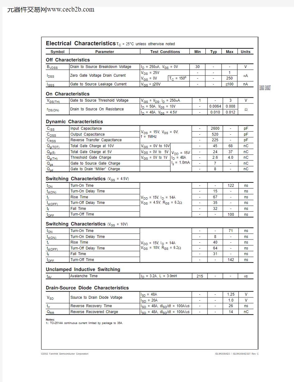
Symbol Parameter
Ratings Units V DSS Drain to Source Voltage 30V V GS
Gate to Source Voltage ±20
V
I D
Drain Current
50A Continuous (T C = 25o C, V GS = 10V) Note 1
Continuous (T C = 100o C, V GS = 4.5V) Note 148A Continuous (T C = 25o C, V GS = 10V, R θJC = 52o C/W)14A Pulsed
Figure 4A P D Power dissipation Derate above 25o C
1000.67W W/o C
T J , T STG
Operating and Storage T emperature
-55 to 175
o
C
R θJC Thermal Resistance Junction to Case TO-252, TO-251 1.5o C/W R θJA Thermal Resistance Junction to Ambient TO-252, TO-251
100o C/W R θJA
Thermal Resistance Junction to Ambient TO-252, 1in 2 copper pad area
52
o
C/W
Device Marking
Device
Package Reel Size Tape Width Quantity N308AD
ISL9N308AD3ST TO-252AA 330mm 16mm
2500 units N308AD
ISL9N308AD3
TO-251AA
T ube
N/A
75 units
D
G
S
G S
D
TO-252D-PAK (TO-252)
G D S
I-PAK (TO-251AA)
Switching Characteristics (V GS = 4.5V)
Switching Characteristics (V GS = 10V)
Unclamped Inductive Switching
Drain-Source Diode Characteristics
Notes:
1:TO-251AA continuous current limited by package to 35A.
C RSS Reverse Transfer Capacitance -225-pF Q g(TOT)Total Gate Charge at 10V V GS = 0V to 10V
V DD = 15V I D = 48A
I g = 1.0mA
-4568nC Q g(5)Total Gate Charge at 5V V GS = 0V to 5V -2437nC Q g(TH)Threshold Gate Charge V GS = 0V to 1V - 2.6 4.0nC Q gs Gate to Source Gate Charge -7-nC Q gd
Gate to Drain “Miller ” Charge
-8
-nC
t ON Turn-On Time V DD = 15V, I D = 14A V GS = 4.5V, R GS = 6.2?
--122ns t d(ON)Turn-On Delay Time -15-ns t r Rise Time
-67-ns t d(OFF)Turn-Off Delay Time -35-ns t f Fall Time -32-ns t OFF
Turn-Off Time
--100
ns
t ON Turn-On Time V DD = 15V, I D = 14A V GS = 10V, R GS = 6.2?
--71ns t d(ON)Turn-On Delay Time -8-ns t r Rise Time
-40-ns t d(OFF)Turn-Off Delay Time -64-ns t f Fall Time -31-ns t OFF
Turn-Off Time
--142
ns
t AV
Avalanche Time
I D = 3.2A, L = 3.0mH
215
--μs
V SD Source to Drain Diode Voltage I SD = 48A -- 1.25V I SD = 20A
-- 1.0V t rr Reverse Recovery Time I SD = 48A, dI SD /dt = 100A/μs --26ns Q RR
Reverse Recovered Charge
I SD = 48A, dI SD /dt = 100A/μs
--14
nC
Figure 1. Normalized Power Dissipation vs
Ambient Temperature
Figure 2. Maximum Continuous Drain Current vs
Case Temperature
Figure 3. Normalized Maximum Transient Thermal Impedance
Figure 4. Peak Current Capability
0.1
1
10-5
10-4
10-3
10-2
10-1
100
101
0.01
2t, RECTANGULAR PULSE DURATION (s)
Z θJ C , N O R M A L I Z E D T H E R M A L I M P E D A N C E
NOTES:
DUTY FACTOR: D = t 1/t 2
PEAK T J = P DM x Z θJC x R θJC + T C
P DM
t 1
t 2
0.50.20.10.050.01
0.02DUTY CYCLE - DESCENDING ORDER SINGLE PULSE
100
1000
10-5
10-4
10-3
10-2
10-1
100
101
40I D M , P E A K C U R R E N T (A )
t, PULSE WIDTH (s)
T C = 25o C
I = I 25
175 - T C 150
FOR TEMPERATURES
ABOVE 25o C DERATE PEAK CURRENT AS FOLLOWS:
V GS = 5V
TRANSCONDUCTANCE MAY LIMIT CURRENT IN THIS REGION
V GS = 10V
Figure 5. Transfer Characteristics
Figure 6. Saturation Characteristics
Figure 7. Drain to Source On Resistance vs Gate
Voltage and Drain Current
Figure 8. Normalized Drain to Source On Resistance vs Junction Temperature
Figure 9. Normalized Gate Threshold Voltage vs
Junction Temperature Figure 10. Normalized Drain to Source Breakdown Voltage vs Junction Temperature
510
15
20
25
2
4
6
8
10
V GS , GATE TO SOURCE VOLTAGE (V)
r D S (O N ), D R A I N T O S O U R C E O N R E S I S T A N C E (m ?)
I D = 14A
I D = 50A
PULSE DURATION = 80μs DUTY CYCLE = 0.5% MAX T C = 25o C
I D = 32A
0.51.0
1.5
2.0
-80
-40
40
80
120
160
200
N O R M A L I Z E D D R A I N T O S O U R C E T J , JUNCTION TEMPERATURE (o C)
O N R E S I S T A N C E
V GS = 10V, I D = 50A
PULSE DURATION = 80μs DUTY CYCLE = 0.5% MAX
0.2
0.40.60.81.01.2
1.4
-80
-40
40
80
120
160
200
N O R M A L I Z E D G A T E T J , JUNCTION TEMPERATURE (o C)
V GS = V DS , I D = 250μA
T H R E S H O L D V O L T A G E
0.91.0
1.1
1.2
-80
-40
40
80
120
160
200
T J
, JUNCTION TEMPERATURE (o C)
N O R M A L I Z E D D R A I N T O S O U R C E B R E A K D O W N V O L T A G E
I D = 250μA
whether there is copper on one side or both sides of the board.2. The number of copper layers and the thickness of the board.3. The use of external heat sinks.4. The use of thermal vias.5. Air flow and board orientation.
6. For non steady state applications, the pulse width, the duty cycle and the transient thermal response of the part,the board and the environment they are in.Fairchild provides thermal information to assist the designer ’s preliminary application evaluation. Figure 21defines the R θJA for the device as a function of the top copper (component side) area. This is for a horizontally positioned FR-4 board with 1oz copper after 1000 seconds of steady state power with no air flow. This graph provides the necessary information for calculation of the steady state junction temperature or power dissipation. Pulse applications can be evaluated using the Fairchild device Spice thermal model or manually utilizing the normalized maximum transient thermal impedance curve.
Displayed on the curve are R θJA values listed in the Electrical Specifications table. The points were chosen to depict the compromise between the copper board area, the thermal resistance and ultimately the power dissipation,P DM .
Thermal resistances corresponding to other copper areas can be obtained from Figure 21 or by calculation using Equation 2. R θJA is defined as the natural log of the area times a coefficient added to a constant. The area, in square inches is the top copper area including the gate and source pads.
(EQ. 2)
R θJA 33.3223.84
0.268Area +()
------------------------------------
+=
MMED 16 6 8 8 MMEDMOD MSTRO 16 6 8 8 MSTROMOD MWEAK 16 21 8 8 MWEAKMOD
RBREAK 17 18 RBREAKMOD 1RDRAIN 50 16 RDRAINMOD 2.5e-3RGATE 9 20 3.4RLDRAIN 2 5 10RLGATE 1 9 45.8RLSOURCE 3 7 14.7
RSLC1 5 51 RSLCMOD 1e-6RSLC2 5 50 1e3
RSOURCE 8 7 RSOURCEMOD 2.55e-3RVTHRES 22 8 RVTHRESMOD 1RVTEMP 18 19 RVTEMPMOD 1S1A 6 12 13 8 S1AMOD S1B 13 12 13 8 S1BMOD S2A 6 15 14 13 S2AMOD S2B 13 15 14 13 S2BMOD VBAT 22 19 DC 1
ESLC 51 50 VALUE={(V(5,51)/ABS(V(5,51)))*(PWR(V(5,51)/(1e-6*200),5))}
.MODEL DBODYMOD D (IS = 1.9e-11 N = 1.075RS = 4.2e-3TRS1 = 9e-4TRS2 = 1e-6 XTI = 2.2CJO = 1.1e-9TT = 8e-11 M = 0.49)
.MODEL DBREAKMOD D (RS = 1.7e-1TRS1 = 1e-3TRS2 = -8.9e-6).MODEL DPLCAPMOD D (CJO = 8.2e-10IS = 1e-30N = 10 M = 0.45)
.MODEL MMEDMOD NMOS (VTO = 1.9 KP = 3 IS=1e-30 N = 10 TOX = 1 L = 1u W = 1u RG = 3.4).MODEL MSTROMOD NMOS (VTO = 2.35KP = 90 IS = 1e-30 N= 10 TOX = 1 L = 1u W = 1u)
.MODEL MWEAKMOD NMOS (VTO = 1.6 KP = 0.05 IS = 1e-30 N = 10 TOX = 1 L = 1u W = 1u RG = 34 RS = 0.1).MODEL RBREAKMOD RES (TC1 = 1e-3TC2 = -7e-7).MODEL RDRAINMOD RES (TC1 = 7e-3TC2 = 1e-5).MODEL RSLCMOD RES (TC1 = 1e-3 TC2 = 1e-6)
.MODEL RSOURCEMOD RES (TC1 = 1e-3 TC2 = 1e-6).MODEL RVTHRESMOD RES (TC1 = -2.7e-3 TC2 = -1e-5).MODEL RVTEMPMOD RES (TC1 = -1.8e-3TC2 = 1e-6).MODEL S1AMOD VSWITCH (RON = 1e-5ROFF = 0.1VON = -4.0VOFF= -0.8).MODEL S1BMOD VSWITCH (RON = 1e-5ROFF = 0.1VON = -0.8VOFF= -4.0).MODEL S2AMOD VSWITCH (RON = 1e-5ROFF = 0.1VON = -0.3VOFF= 0.2).MODEL S2BMOD VSWITCH (RON = 1e-5ROFF = 0.1VON = 0.2VOFF= -0.3)
.ENDS
For further discussion of the PSPICE model, consult A New PSPICE Sub-Circuit for the Power MOSFET Featuring Global Temperature Options; IEEE Power Electronics Specialist Conference Records, 1991, written by William J. Hepp and C. Frank Wheatley.
68
58
+-RBREAK
RVTEMP VBAT RVTHRES
IT
17
181922
121315
S1A S1B
S2A S2B
CA
CB EGS
EDS
14
8
138
1413RSOURCE
7
3
RLSOURCE
8
+-+
-
dp.dplcap n10 n5 = model=dplcapmod i.it n8 n17 = 1
l.ldrain n2 n5 = 1e-9l.lgate n1 n9 = 4.58e-9l.lsource n3 n7 = 1.47e-9
m.mmed n16 n6 n8 n8 = model=mmedmod, l=1u, w=1u m.mstrong n16 n6 n8 n8 = model=mstrongmod, l=1u, w=1u m.mweak n16 n21 n8 n8 = model=mweakmod, l=1u, w=1u res.rbreak n17 n18 = 1, tc1 = 1e-3, tc2 = -7e-7res.rdrain n50 n16 = 2.5e-3, tc1 = 7e-3, tc2 = 1e-5res.rgate n9 n20 = 3.4res.rldrain n2 n5 = 10res.rlgate n1 n9 = 45.8res.rlsource n3 n7 = 14.7
res.rslc1 n5 n51= 1e-6, tc1 = 1e-3, tc2 = 1e-6res.rslc2 n5 n50 = 1e3
res.rsource n8 n7 = 2.55e-3, tc1 = 1e-3, tc2 = 1e-6res.rvtemp n18 n19 = 1, tc1 = -1.8e-3, tc2 = 1e-6res.rvthres n22 n8 = 1, tc1 = -2.7e-3, tc2 = -1e-5spe.ebreak n11 n7 n17 n18 = 32.7spe.eds n14 n8 n5 n8 = 1spe.egs n13 n8 n6 n8 = 1spe.esg n6 n10 n6 n8 = 1
spe.evtemp n20 n6 n18 n22 = 1spe.evthres n6 n21 n19 n8 = 1
sw_vcsp.s1a n6 n12 n13 n8 = model=s1amod sw_vcsp.s1b n13 n12 n13 n8 = model=s1bmod sw_vcsp.s2a n6 n15 n14 n13 = model=s2amod sw_vcsp.s2b n13 n15 n14 n13 = model=s2bmod v.vbat n22 n19 = dc=1
equations {
i (n51->n50) +=iscl
iscl: v(n51,n50) = ((v(n5,n51)/(1e-9+abs(v(n5,n51))))*((abs(v(n5,n51)*1e-6/200))** 5))}}
1822+-6
8
+
-198
+-17186858
+
-RBREAK RVTEMP
VBAT RVTHRES
IT
17
181922
121315
S1A S1B S2A S2B
CA
CB EGS
EDS
14
8
13
81413MWEAK EBREAK
DBODY
RSOURCE
SOURCE
11
7
3
LSOURCE RLSOURCE CIN
RDRAIN
EVTHRES 16
218
MMED
MSTRO
1
GATE RGATE EVTEMP
9ESG
LGATE
RLGATE
20
+-+-+-6
template thermal_model th tl thermal_c th, tl {
ctherm.ctherm1 th 6 = 2.0e-4ctherm.ctherm2 6 5 = 3.0e-3ctherm.ctherm3 5 4 = 3.4e-3ctherm.ctherm4 4 3 = 4.0e-3ctherm.ctherm5 3 2 = 1.0e-2ctherm.ctherm6 2 tl = 5.0e-2rtherm.rtherm1 th 6 = 1.5e-3rtherm.rtherm2 6 5 = 5.5e-3rtherm.rtherm3 5 4 = 5.2e-2rtherm.rtherm4 4 3 = 3.5e-1rtherm.rtherm5 3 2 = 3.8e-1rtherm.rtherm6 2 tl = 4.1e-1}
RTHERM4RTHERM6RTHERM5CTHERM4
CTHERM6
CTHERM5
tl 2
3
4
CASE
TRADEMARKS
The following are registered and unregistered trademarks Fairchild Semiconductor owns or is authorized to use and is not intended to be an exhaustive list of all such trademarks.
ACEx?Bottomless?CoolFET?CROSSVOLT?DOME?EcoSPARK?
E2CMOS?EnSigna?
FACT?
FACT Quiet Series?FAST?
FASTr?FRFET?
GlobalOptoisolator?
GTO?
HiSeC?
I2C?
ISOPLANAR?
LittleFET?
MicroFET?
MicroPak?
MICROWIRE?
OPTOLOGIC?
OPTOPLANAR?
PACMAN?
POP?
Power247?
PowerTrench?
QFET?
QS?
QT Optoelectronics?
Quiet Series?
SILENT SWITCHER?
SMART START?
SPM?
Stealth?
SuperSOT?-3
SuperSOT?-6
SuperSOT?-8
SyncFET?
TinyLogic?
TruTranslation?
UHC?
UltraFET?
VCX?
DISCLAIMER
FAIRCHILD SEMICONDUCTOR RESERVES THE RIGHT TO MAKE CHANGES WITHOUT FURTHER NOTICE TO ANY PRODUCTS HEREIN TO IMPROVE RELIABILITY, FUNCTION OR DESIGN. FAIRCHILD DOES NOT ASSUME ANY LIABILITY ARISING OUT OF THE APPLICATION OR USE OF ANY PRODUCT OR CIRCUIT DESCRIBED HEREIN; NEITHER DOES IT CONVEY ANY LICENSE UNDER ITS PATENT RIGHTS, NOR THE RIGHTS OF OTHERS.
LIFE SUPPORT POLICY
FAIRCHILD’S PRODUCTS ARE NOT AUTHORIZED FOR USE AS CRITICAL COMPONENTS IN LIFE SUPPORT DEVICES OR SYSTEMS WITHOUT THE EXPRESS WRITTEN APPROVAL OF FAIRCHILD SEMICONDUCTOR CORPORATION.
As used herein:
1. Life support devices or systems are devices or systems which, (a) are intended for surgical implant into the body, or (b) support or sustain life, or (c) whose failure to perform when properly used in accordance with instructions for use provided in the labeling, can be reasonably expected to result in significant injury to the user.
2. A critical component is any component of a life support device or system whose failure to perform can be reasonably expected to cause the failure of the life support device or system, or to affect its safety or effectiveness.
PRODUCT STATUS DEFINITIONS
Definition of Terms
Datasheet Identification Product Status Definition
Advance Information Formative or In
Design This datasheet contains the design specifications for product development. Specifications may change in any manner without notice.
Preliminary First Production This datasheet contains preliminary data, and
supplementary data will be published at a later date.
Fairchild Semiconductor reserves the right to make
changes at any time without notice in order to improve
design.
No Identification Needed Full Production This datasheet contains final specifications. Fairchild
Semiconductor reserves the right to make changes at
any time without notice in order to improve design. Obsolete Not In Production This datasheet contains specifications on a product
that has been discontinued by Fairchild semiconductor.
The datasheet is printed for reference information only.