RD15HVF1

OUTLINE DRAWING
note(3)
:Copper of the ground work is exposed in case of frame separation.
note:
(1)Torelance of no designation means typical value. Dimension in mm.(3)
(2):Dipping area
PINS 1:GATE 2:SOURCE 3:DRAIN
4:FIN(SOURCE)
12
3
4
DESCRIPTION
RD15HVF1 is a MOS FET type transistor specifically designed for VHF/UHF High power amplifiers applica -tions.
FEATURES
High power and High Gain:
Pout>15W, Gp>14dB @Vdd=12.5V,f=175MHz Pout>15W, Gp>7dB @Vdd=12.5V,f=520MHz High Efficiency: 60%typ. on VHF Band High Efficiency: 55%typ. on UHF Band
APPLICATION
For output stage of high power amplifiers in VHF/UHF Band mobile radio sets.
RoHS COMPLIANT
RD15HVF1-101 is a RoHS compliant products. RoHS compliance is indicate by the letter “G” after the lot marking.
This product include the lead in high melting temperature type solders. How ever,it applicable to the following exceptions of RoHS Directions.
1.Lead in high melting temperature type solders(i.e.tin-lead solder alloys containing more than85% lead.)
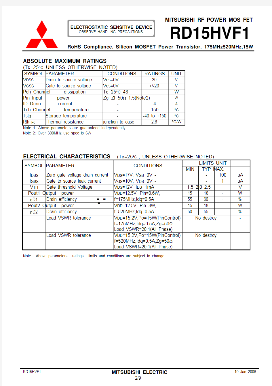
ABSOLUTE MAXIMUM RATINGS
(Tc=25°C UNLESS OTHERWISE NOTED)
SYMBOL PARAMETER CONDITIONS RATINGS UNIT V DSS Drain to source voltage Vgs=0V 30 V V GSS Gate to source voltage Vds=0V +/-20 V Pch Channel dissipation Tc =
25°C 48 W
Pin Input power Zg =Zl =50? 1.5(Note2)
W ID Drain current - 4 A Tch Channel temperature - 150 °C
Tstg Storage temperature - -40 to +150
°C Rth j-c Thermal resistance junction to case 2.6
°C/W Note 1: Above parameters are guaranteed independently.
Note 2: Over 300MHz use spec is 6W
ELECTRICAL CHARACTERISTICS (Tc=25°C , UNLESS OTHERWISE NOTED)
LIMITS UNIT SYMBOL PARAMETER
CONDITIONS
MIN TYP MAX.
I DSS Zero gate voltage drain current V DS =17V, V GS =
0V - - 100 uA I GSS Gate to source leak current V GS =10V, V DS =0V - - 1 uA V TH Gate threshold Voltage V DS =12V, I DS =
1mA 1.5 2.0 2.5 V Pout1 Output power V DD =12.5V, Pin=0.6W, 15 18 - W
ηD1 Drain efficiency
f=175MHz,Idq=0.5A 55 60 - % Pout2 Output power V DD =12.5V, Pin=3W, 15 18 - W
ηD2 Drain efficiency
f=520MHz,Idq=0.5A 50 55 - % Load VSWR tolerance V DD =15.2V,Po=15W(PinControl)
f=175MHz,Idq=0.5A,Zg=50? Load VSWR=20:1(All Phase)
No destroy - Load VSWR tolerance V DD =15.2V,Po=15W(PinControl)
f=520MHz,Idq=0.5A,Zg=50? Load VSWR=20:1(All Phase)
No destroy - Note : Above parameters , ratings , limits and conditions are subject to change.
TYPICAL CHARACTERISTICS
TYPICAL CHARACTERISTICS
TYPICAL CHARACTERISTICS
TEST CIRCUIT(f=175MHz)
L3:4Turns,I.D6mm,D1.6mm P=1 silver plateted copper wire
micro strip line width=4.2mm/50OHM,er:2.7,t=1.6mm Note:Board material-Teflon substrate
C1:2200pF 10uF in parallel RF-OUT
L1:4Turns,I.D6mm,D1.6mm P=1 silver plateted copper wire Vgg
Vdd
Dimensions:mm
C2:2200pF*2 in parallel
C3:2200pF,330uF in parallel
L2:5Turns,I.D6mm,D1.6mm P=1 silver plateted copper wire
TEST CIRCUIT(f=520MHz)
L2:2Turns,I.D6mm,D1.6mm P=1 silver plateted copper wire C3:2200pF,330uF in parallel
C2:2200pF*2 in parallel Dimensions:mm
Vdd
Vgg
L1:4Turns,I.D6mm,D1.6mm P=1 silver plateted copper wire C1:2200pF 10uF in parallel Note:Board material-Teflon substrate
micro strip line width=4.2mm/50OHM,er:2.7,t=1.6mm L3:4Turns,I.D6mm,D1.6mm P=1 silver plateted copper wire
INPUT/OUTPUT IMPEDANCE VS.FREQUENCY CHARACTERISTICS
f=520MHz Zout
f=520MHz Zin
f=175MHz Zout
Zo=50ohm
f=175MHz Zin
Zin , Zout
f Zin Zout
(MHz) (ohm) (ohm) Conditions
Po=15W, Vdd=12.5V,Pin=0.6W 175 2.34-j8.01 3.06+j0.74
Po=15W, Vdd=12.5V,Pin=3.0W 520 5.42+j9.22 6.02+j12.34