2N6509中文资料
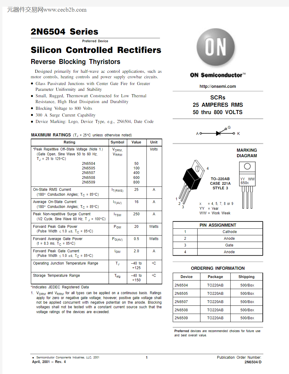

2N6504 Series
Preferred Device
Silicon Controlled Rectifiers
Reverse Blocking Thyristors
Designed primarily for half-wave ac control applications, such as motor controls, heating controls and power supply crowbar circuits.?Glass Passivated Junctions with Center Gate Fire for Greater Parameter Uniformity and Stability
?Small, Rugged, Thermowatt Constructed for Low Thermal Resistance, High Heat Dissipation and Durability ?Blocking V oltage to 800 V olts ?300 A Surge Current Capability
?Device Marking: Logo, Device Type, e.g., 2N6504, Date Code
MAXIMUM RATINGS (T
= 25°C unless otherwise noted)
1.V DRM and V RRM for all types can be applied on a continuous basis. Ratings apply for zero or negative gate voltage; however, positive gate voltage shall not be applied concurrent with negative potential on the anode. Blocking voltages shall not be tested with a constant current source such that the voltage ratings of the devices are exceeded.
Preferred devices are recommended choices for future use and best overall value.
Device Package Shipping ORDERING INFORMATION
2N6504TO220AB 500/Box 2N6505TO220AB 2N6507TO220AB https://www.wendangku.net/doc/41470303.html,
500/Box 500/Box 2N6508TO220AB 500/Box 2N6509
TO220AB
500/Box
*THERMAL CHARACTERISTICS
ELECTRICAL CHARACTERISTICS (T = 25°C unless otherwise noted.)
OFF CHARACTERISTICS
ON CHARACTERISTICS
DYNAMIC CHARACTERISTICS
2.Pulse Test: Pulse Width ≤ 300 μs, Duty Cycle ≤ 2%.
+ Current
Symbol
Parameter
V DRM Peak Repetitive Off State Forward Voltage I DRM Peak Forward Blocking Current
V RRM Peak Repetitive Off State Reverse Voltage I RRM Peak Reverse Blocking Current V TM Peak On State Voltage I H
Holding Current
Voltage Current Characteristic of SCR
C T , M A X I M U M C A S E T E M P E R A T U
R E ( C )
°I T(AV), ON?STATE FORWARD CURRENT (AMPS)
P , A V E R A G E P O W E R (W A
T T S )(A V
)I T(AV), AVERAGE ON?STATE FORWARD CURRENT (AMPS)
Figure 1. Average Current Derating Figure 2. Maximum On–State Power Dissipation
1.00.020.030.050.070.1
0.20.30.50.70.01
t, TIME (ms)
r (t ), T R A N S I E N T T H E R M A L R E S I S T A N C E (N O R M A L I Z E D )
F
i , I N S T A N T A N E O U S F O R W A R D C U R R E N T (A M P S )Figure 5. Thermal Response
TYPICAL TRIGGER CHARACTERISTICS
Figure 6. Typical Gate Trigger Current
versus Junction Temperature Figure 7. Typical Gate Trigger Voltage
versus Junction Temperature
Figure 8. Typical Holding Current versus Junction Temperature
10
1
100
125
110806550355-10
-25
20T J , JUNCTION TEMPERATURE (°C)
I G T , G A T E T R I G G E R C U R R E N T (m A )
-4095
V G T 125
11095
80
50
35
5
-400.8-10
-2520
T J , JUNCTION TEMPERATURE (°C)
0.60.40.2
, G A T E T R I G G E R V O
L T A G E (V O L T S )
1.065
0.90.70.50.3
I , H O L D I N G C U R R E N T (m A )
H T J , JUNCTION TEMPERATURE (°C)
100
10
1
125
110958050355-40-10
-252065
PACKAGE DIMENSIONS
TO–220AB
CASE 221A–07
ISSUE AA
STYLE 3:
PIN 1.CATHODE
2.ANODE
3.GATE
4.ANODE
Notes
ON Semiconductor and are trademarks of Semiconductor Components Industries, LLC (SCILLC). SCILLC reserves the right to make changes without further notice to any products herein. SCILLC makes no warranty, representation or guarantee regarding the suitability of its products for any particular purpose, nor does SCILLC assume any liability arising out of the application or use of any product or circuit, and specifically disclaims any and all liability, including without limitation special, consequential or incidental damages. “Typical” parameters which may be provided in SCILLC data sheets and/or specifications can and do vary in different applications and actual performance may vary over time. All operating parameters, including “Typicals” must be validated for each customer application by customer’s technical experts. SCILLC does not convey any license under its patent rights nor the rights of others.
SCILLC products are not designed, intended, or authorized for use as components in systems intended for surgical implant into the body, or other applications intended to support or sustain life, or for any other application in which the failure of the SCILLC product could create a situation where personal injury or death may occur. Should Buyer purchase or use SCILLC products for any such unintended or unauthorized application, Buyer shall indemnify and hold SCILLC and its officers, employees, subsidiaries, affiliates, and distributors harmless against all claims, costs, damages, and expenses, and reasonable attorney fees arising out of, directly or indirectly, any claim of personal injury or death associated with such unintended or unauthorized use, even if such claim alleges that SCILLC was negligent regarding the design or manufacture of the part. SCILLC is an Equal Opportunity/Affirmative Action Employer. PUBLICATION ORDERING INFORMATION
CENTRAL/SOUTH AMERICA:
Spanish Phone:303–308–7143 (Mon–Fri 8:00am to 5:00pm MST)
Email:ONlit–spanish@https://www.wendangku.net/doc/41470303.html,
Toll–Free from Mexico: Dial 01–800–288–2872 for Access –
then Dial 866–297–9322
ASIA/PACIFIC: LDC for ON Semiconductor – Asia Support
Phone:1–303–675–2121 (Tue–Fri 9:00am to 1:00pm, Hong Kong Time)
Toll Free from Hong Kong & Singapore:
001–800–4422–3781
Email: ONlit–asia@https://www.wendangku.net/doc/41470303.html,
JAPAN: ON Semiconductor, Japan Customer Focus Center
4–32–1 Nishi–Gotanda, Shinagawa–ku, Tokyo, Japan 141–0031
Phone: 81–3–5740–2700