CPWR-AN10 碳化硅MOS管驱动电路

C P W R -A N 10, R E V A S i C M O S F E T I s
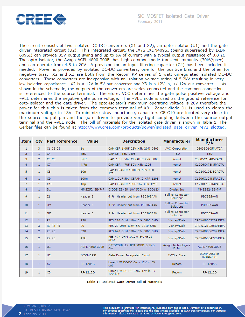
o l a t e d G a t e D r i v e r - F e b r u a r y 2011 Figure 1: Isolated Gate Driver Top View Figure 2: Isolated Gate Driver Bottom View
R220
1210
R420
1210
R520
1210X 2
RP-1205C
+VIN
1
-VIN
2
-VOUT
5
+VOUT
7
U1ACPL-4800-300E
NC
1ANODE 2CATH 3NC
4
VCC
8NC 7VO 6GND
5
C810n 1210
D1
MMSZ5248B-7-F
C74.7u 1206
C1010u 1210
X 3
RP-1212D
+VIN
1
-VIN
2
-VOUT
5
COM
6+VOUT 7-VEE
-VEE
-VEE
R3620
0805-VEE
-VEE
-VEE
THESE COMPONENTS ARE LOCATED ON THE -VEE PLANE
0.100" ISOLATION BOUNDRY SLIT BOARD IF REQ.
+VCC
+VCC
R6620
0805
C6100n 0805
C4TBD 0805
C9100n
VCC HIGH
VCC HIGH RTN INPUT HIGH
U2IXDN409SI
VCC 1IN 2NC
3GND 4
VCC 8OUT 7OUT
6GND 5
INPUT LOW VCC LOW
SiC MOSFET Isolated Gate Driver
February 2011
The circuit consists of two isolated DC-DC converters (X1 and X2), an opto-isolator (U1) and the gate driver integrated circuit (U2). This integrated circuit, the IXYS IXDN409SI (being superseded by IXDN 609SI) can provide 35V output swing and up to 9A of current with a typical output resistance of 0.8 Ω. The opto-isolator , the Avago ACPL-4800-300E, has high common mode transient immunity (30kV/μsec) and can operate from 4.5 to 20V . A provision for an input filtering capacitor (C4) has been included if needed. Power is provided by isolated DC-DC converters; one for the positive bias and the other for negative bias. X2 and X3 are both from the Recom RP series of 1 watt unregulated isolated DC-DC converters. These converters are inexpensive with an isolation voltage rating of 5.2kV resulting in very low isolation capacitance. X2 is a 12V in 5V out converter and X3 is a 12V in, +/-12V out converter . As shown in the schematic, the outputs of the converters are series connected and the common connection is referenced to the source terminal. Therefore, VCC determines the gate pulse positive voltage and –VEE determines the negative gate pulse voltage. The –VEE node is used as the ground reference for opto-isolator and the gate driver . The opto-isolator’s maximum operating voltage is 20V therefore the power for this chip is taken from the common terminal of X3. Zener diode D1 is used to clamp the maximum voltage to 18V . To minimize stray inductance, capacitors C8-C10 are located very close to the source output pin and the gate driver to provide very tight coupling between the source output terminal and the –VEE node. The bill of materials for the isolated gate driver is shown in Table 1. The Gerber files can be found at https://www.wendangku.net/doc/4b1663495.html,/products/power/isolated_gate_driver_rev2_slotted.
Table 1: Isolated Gate Driver Bill of Materials
SiC MOSFET Isolated Gate Driver
February 2011
Operation of the gate driver is as follows. A +10 to +12V pulse is applied to the opto causes the gate terminal to go high. The intent of this circuit is to afford the maximum flexibility. Therefore, unregulated DC-DC converters were used so that the output gate pulse positive and negative voltage levels can be adjusted at ground level. The gate voltage positive level is adjusted by varying the voltage between the VCC HIGH and VCC HIGH RTN and the negative pulse level is adjusted by varying the voltage between the VCC LOW and VCC LOW RTN pins. Care must be taken during adjustment to insure that the voltage between the VCC and –VEE nodes does not exceed the maximum ratings of U2, which is 35V.
The circuit can be modified to remove the isolated DC-DC converters to allow direct connection of VCC, source, and –VEE directly to external power supplies. This is accomplished by removing the converters and placing jumpers and an additional 1k resistor. The schematic of this change is shown in Figure 4.
Figure 4: Modified Isolated Gate Driver Schematic
As shown, the modifications are chiefly jumpers to bypass the DC-DC converters. The common terminal is now floating so a new resistor (R9) is required to supply power to the opto-isolator. This resistor has been selected for a +20V/-2V gate pulse suitable for low duty cycle double pulse testing. Lower voltage gate pulses might require this resistor to be changed to a different value. The pictures in Figure 5 show how the jumpers and R9 are installed.
R9
Figure 5: Isolated Gate Driver Modifications to Remove DC-DC Converters