UCC28070PWR中文资料

FEATURES APPLICATIONS
DESCRIPTION
UCC28070
SLUS794A–NOVEMBER2007–REVISED MARCH2008 https://www.wendangku.net/doc/4e15519784.html,
Interleaving Continuous Conduction Mode PFC Controller
?High-Efficiency Server and Desktop Power ?Interleaved Average Current-Mode PWM
Supplies
Control with Inherent Current Matching
?Telecom Rectifiers
?Advanced Current Synthesizer Current
Sensing for Superior Efficiency
?Highly-Linear Multiplier Output with Internal
The UCC28070is an advanced power factor Quantized Voltage Feed-Forward Correction
correction device that integrates two pulse-width for Near-Unity PF
modulators(PWMs)operating180°out of phase.?Programmable Frequency(10kHz to300kHz)
This interleaved PWM operation generates ?Programmable Maximum Duty-Cycle Clamp substantial reduction in the input and output ripple
currents,and the conducted-EMI filtering becomes ?Programmable Frequency Dithering Rate and
easier and less expensive.A significantly improved Magnitude for Enhanced EMI Reduction
multiplier design provides a shared current reference –Magnitude:3kHz to30kHz
to two independent current amplifiers that ensures –Rate:Up to30kHz matched average current mode control in both PWM
outputs while maintaining a stable,low-distortion ?External Clock Synchronization Capability
sinusoidal input line current.
?Enhanced Load and Line Transient Response
through Voltage Amplifier Output Slew-Rate The UCC28070contains multiple innovations
including current synthesis and quantized voltage Correction
feed-forward to promote performance enhancements ?Programmable Peak Current Limiting
in PF,efficiency,THD,and transient response.?Bias-Supply UVLO,Over-Voltage Protection,Features including frequency dithering,clock Open-Loop Detection,and PFC-Enable synchronization,and slew rate enhancement further Monitoring expand the potential performance enhancements.?External PFC-Disable Interface The UCC28070also contains a variety of protection ?Open-Circuit Protection on VSENSE and features including output over-voltage detection, VINAC pins programmable peak-current limit,under-voltage
lockout,and open-loop protection.?Programmable Soft Start
?20-Lead TSSOP Package
Simplified Application Diagram
Please be aware that an important notice concerning availability,standard warranty,and use in critical applications of
Texas Instruments semiconductor products and disclaimers thereto appears at the end of this data sheet.
https://www.wendangku.net/doc/4e15519784.html,
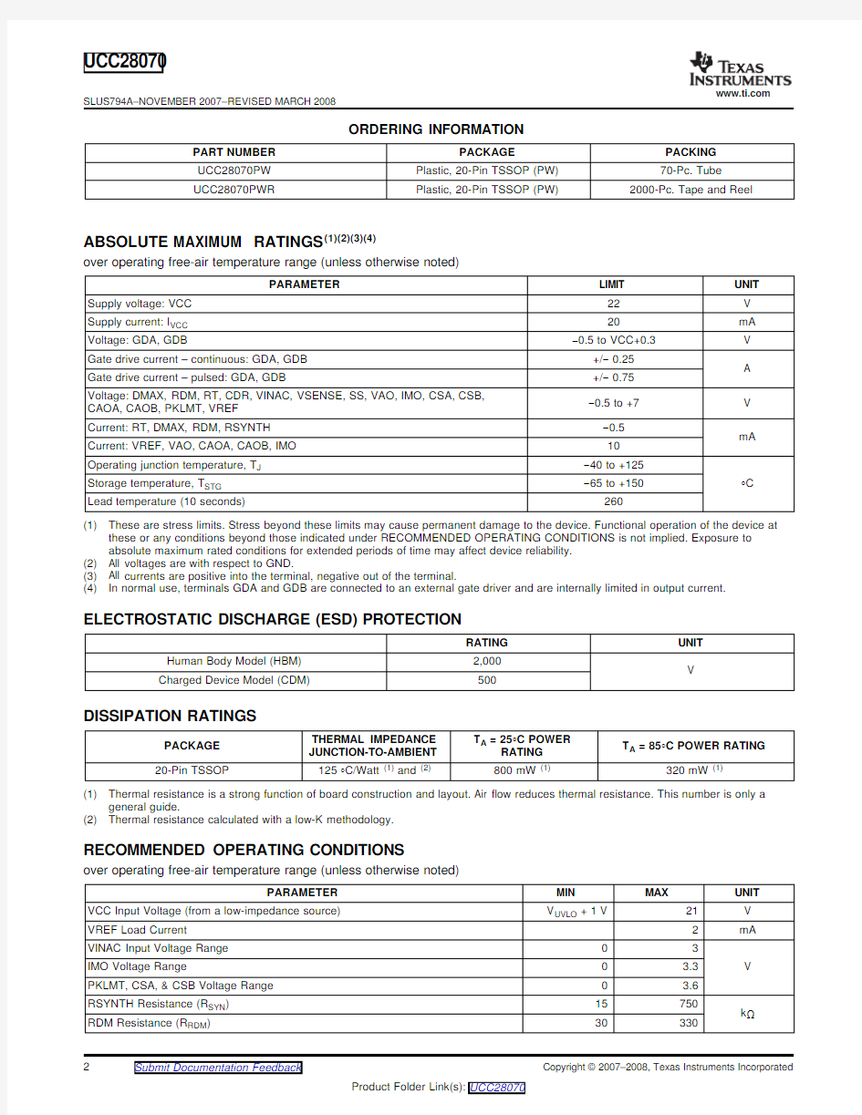
ABSOLUTE MAXIMUM RATINGS (1)(2)(3)(4)
ELECTROSTATIC DISCHARGE (ESD)PROTECTION
DISSIPATION RATINGS
RECOMMENDED OPERATING CONDITIONS
UCC28070
SLUS794A–NOVEMBER 2007–REVISED MARCH 2008
ORDERING INFORMATION
PART NUMBER PACKAGE
PACKING UCC28070PW Plastic,20-Pin TSSOP (PW)70-Pc.Tube UCC28070PWR
Plastic,20-Pin TSSOP (PW)
2000-Pc.Tape and Reel
over operating free-air temperature range (unless otherwise noted)
PARAMETER
LIMIT UNIT Supply voltage:VCC 22V Supply current:I VCC 20
mA Voltage:GDA,GDB
?0.5to VCC+0.3
V Gate drive current –continuous:GDA,GDB +/?0.25A Gate drive current –pulsed:GDA,GDB
+/?0.75Voltage:DMAX,RDM,RT,CDR,VINAC,VSENSE,SS,VAO,IMO,CSA,CSB,?0.5to +7V CAOA,CAOB,PKLMT,VREF Current:RT,DMAX,RDM,RSYNTH ?0.5mA
Current:VREF,VAO,CAOA,CAOB,IMO 10Operating junction temperature,T J ?40to +125Storage temperature,T STG ?65to +150
°C Lead temperature (10seconds)260
(1)These are stress limits.Stress beyond these limits may cause permanent damage to the device.Functional operation of the device at these or any conditions beyond those indicated under RECOMMENDED OPERATING CONDITIONS is not implied.Exposure to absolute maximum rated conditions for extended periods of time may affect device reliability.(2)All voltages are with respect to GND.
(3)All currents are positive into the terminal,negative out of the terminal.
(4)
In normal use,terminals GDA and GDB are connected to an external gate driver and are internally limited in output current.
RATING
UNIT Human Body Model (HBM)2,000V
Charged Device Model (CDM)
500
THERMAL IMPEDANCE T A =25°C POWER
PACKAGE T A =85°C POWER RATING
JUNCTION-TO-AMBIENT RATING
20-Pin TSSOP
125°C/Watt
(1)
and
(2)
800mW
(1)
320mW
(1)
(1)Thermal resistance is a strong function of board construction and layout.Air flow reduces thermal resistance.This number is only a general guide.
(2)
Thermal resistance calculated with a low-K methodology.
over operating free-air temperature range (unless otherwise noted)
PARAMETER
MIN MAX
UNIT VCC Input Voltage (from a low-impedance source)V UVLO +1V
21V VREF Load Current 2mA
VINAC Input Voltage Range 03IMO Voltage Range
0 3.3V PKLMT,CSA,&CSB Voltage Range 0 3.6RSYNTH Resistance (R SYN )15750k ΩRDM Resistance (R RDM )
30
330
https://www.wendangku.net/doc/4e15519784.html,
ELECTRICAL CHARACTERISTICS
UCC28070 SLUS794A–NOVEMBER2007–REVISED MARCH2008
over operating free-air temperature range?40°C Bias Supply VCC SHUNT VCC shunt voltage(1)I VCC=10mA232527V VCC current,disabled VSENSE=0V7 mA VCC current,enabled VSENSE=3V(switching)912 VCC=7V200μA VCC current,UVLO VCC=9V46mA V UVLO UVLO turn-on threshold Measured at VCC(rising)9.810.210.6 UVLO hysteresis Measured at VCC(falling)1V VREF enable threshold Measured at VCC(rising)7.588.5 Linear Regulator VREF voltage,no load I VREF=0mA 5.826 6.18V Measured as the change in VREF, VREF load rejection-1212 (I VREF=0mA and?2mA) mV Measured as the change in VREF, VREF line rejection-1212 (VCC=11V and20V,I VREF=0μA) PFC Enable V EN Enable threshold Measured at VSENSE(rising)0.650.750.85 V Enable hysteresis0.15 External PFC Disable Disable threshold Measured at SS(falling)0.50.6 V Hysteresis VSENSE>0.85V0.15 Oscillator Output phase shift Measured between GDA and GDB179180181Degree V DMAX,V RT, Timing regulation voltages Measured at DMAX,RT,&RDM 2.913 3.09V and V RDM R RT=750k?,R DMX=681k?, 9.51010.5 V RDM=0V,V CDR=6V R RT=75k?,R DMX=68.1k?, f PWM PWM switchin g frequency95100105kHz V RDM=0V,V CDR=6V R RT=24.9k?,R DMX=22.6k?, 270290330 V RDM=0V,V CDR=6V R RT=75k?,R DMX=68.1k?, D MAX Duty-cycle clamp92%95%98% V RDM=0V,V CDR=6V R RT=24.9k?,R DMX=22.6k?, Minimum programmable off-time50150250ns V RDM=0V,V CDR=6V R RDM=316k?,R RT=75k?234 Frequency dithering magnitude change f DM in f PWM R RDM =31.6k?,R RT=24.9k?243036 kHz C CDR=2.2nF,R RDM=100k?3 Frequency dithering rate rate of f DR change in f PWM C CDR =0.3nF,R RDM=100k?20 Dither rate current Measure at CDR(sink and source)10μA I CDR Dither disable threshold Measured at C CDR(rising)5 5.25V (1)Excessive VCC input voltage and/or current damages the device.This clamp will not protect the device from an unregulated supply.If an unregulated supply is used,a series-connected fixed positive voltage regulator such as a UA78L15A is recommended.See the Absolute Maximum Ratings section for the limits on VCC voltage and current. https://www.wendangku.net/doc/4e15519784.html, UCC28070 SLUS794A–NOVEMBER 2007–REVISED MARCH 2008 ELECTRICAL CHARACTERISTICS (continued) over operating free-air temperature range ?40°C SYMBOL PARAMETER TEST CONDITIONS MIN TYP MAX UNITS Clock Synchronization V CDR SYNC enable threshold Measured at CDR (rising) 5 5.25V V CDR =6V,Measured from RDM (rising)to SYNC propagation delay 50100ns GDx (rising) SYNC threshold (Rising)V CDR =6V,Measured at RDM 1.2 1.5 V SYNC threshold (Falling)V CDR =6V,Measured at RDM 0.40.7Positive pulse width 0.2 μs SYNC pulses Maximum duty cycle (2) 50 % Voltage Amplifier VSENSE voltage In regulation,T A =25°C 2.973 3.03V VSENSE voltage In regulation 2.94 3 3.06VSENSE input bias current In regulation 250500nA VAO high voltage VSENSE =2.9V 4.85 5.2V VAO low voltage VSENSE =3.1V 0.050.50 g MV VAO transconductance 2.8V 3.2V,VAO =3V 70μS VAO sink current,overdriven limit VSENSE =3.5V,VAO =3V 30VAO source current,overdriven VSENSE =2.5V,VAO =3V,SS =3V ?30μA VAO source current,VSENSE =2.5V,VAO =3V ?130overdriven limit +I SRC Measured as VSENSE (falling)/VSENSE Slew-rate correction threshold 929395%(regulation) Slew-rate correction hysteresis Measured at VSENSE (rising)39 mV Measured at VAO,in addition to VAO I SRC Slew-rate correction current ?100 μA source current.Slew-rate correction enable threshold Measured at SS (rising)4V VAO discharge current VSENSE =0.5V,VAO =1V 10 μA Soft Start I SS SS source current VSENSE =0.9V,SS =1V ?10μA Adaptive source current VSENSE =2.0V,SS =1V ?1.5-2.5mA Adaptive SS disable Measured as VSENSE –SS -30030 mV SS sink current VSENSE =0.5V,SS =0.2V 0.5 0.9 mA (2) Due to the influence of the synchronization pulse width on the programmability of the maximum PWM switching duty cycle (D MAX )it is recommended to minimize the synchronization signal's duty cycle. https://www.wendangku.net/doc/4e15519784.html, UCC28070 SLUS794A–NOVEMBER2007–REVISED MARCH2008 ELECTRICAL CHARACTERISTICS(continued) over operating free-air temperature range?40°C Over Voltage Measured as VSENSE(rising)/VSENSE V OVP OVP threshold104106108% (regulation) OVP hysteresis Measured at VSENSE(falling)100mV Measured between VSENSE(rising)and OVP propagation delay0.20.3μs GDx(falling) Zero-Power V ZPWR Zero-power detect threshold Measured at VAO(falling)0.650.75 V Zero-power hysteresis0.15 Multiplier VAO≥1.5V,T A=25°C161718 VAO=1.2V,T A=25°C14.517.019.5 k MULT Gain constant VAO≥1.5V151719 μA VAO=1.2V131721 VINAC=0.9V PK,VAO=0.8V-0.200.2 I IMO Output current:zero VINAC=0V,VAO=5V-0.200.2 Quantized Voltage Feed Forward V LVL1Level1threshold(3)0.60.70.8 V LVL2Level2threshold1 V LVL3Level3threshold 1.2 V LVL4Level4threshold 1.4 Measured at VINAC(rising)V V LVL5Level5threshold 1.65 V LVL6Level6threshold 1.95 V LVL7Level7threshold 2.25 V LVL8Level8threshold 2.6 Current Amplifiers CAOx high voltage 5.756 V CAOx low voltage0.1 g MC CAOx transconductance100μS CAOx sink current,overdriven50 μA CAOx source current,overdriven?50 Input common mode range0 3.6V Input offset voltage0?8?20 mV Measured as Phase A’s input offset minus Phase mismatch-12012 Phase B’s input offset CAOx pull-down current VSENSE=0.5V,CAOx=0.2V0.50.9mA (3)The Level1threshold represents the“zero-crossing detection”threshold above which VINAC must rise to initiate a new input half-cycle, and below which VINAC must fall to terminate that half-cycle. https://www.wendangku.net/doc/4e15519784.html, DEVICE INFORMATION GDB SS RT CAOB GND VCC GDA DMAX 123456789201918171615141312VAO RDM PKLMT RSYNTH CSA VSENSE VINAC IMO CDR 10 CSB VREF CAOA 11 UCC28070 SLUS794A–NOVEMBER 2007–REVISED MARCH 2008 ELECTRICAL CHARACTERISTICS (continued) over operating free-air temperature range ?40°C SYMBOL PARAMETER TEST CONDITIONS MIN TYP MAX UNITS Current Synthesizer VSENSE =3V,VINAC =0V 2.913 3.09V RSYNTH Regulation voltage VSENSE =3V,VINAC =2.85V 0.10 0.150.20V Synthesizer disable threshold Measured at RSYNTH (rising) 5 5.25VINAC input bias current 0.250 0.500 μA Peak Current Limit Peak current limit threshold PKLMT =3.30V,measured at CSx (rising) 3.27 3.3 3.33V Measured between CSx (rising)and GDx Peak current limit propagation delay 60 100 ns (falling)edges PWM Ramp V RMP PWM ramp amplitude 3.8 4.0 4.2 V PWM ramp offset voltage T A =25°C,R RT =75k ? 0.65 0.7PWM ramp offset temperature ?2 mV/°C coefficient Gate Drive GDA,GDB output voltage,high,VCC =20V,C LOAD =1nF 11.51315 clamped V GDA,GDB output voltage,High C LOAD =1nF 10 10.5GDA,GDB output voltage,Low C LOAD =1nF 0.20.3Rise time GDx 1V to 9V,C LOAD =1nF 1830ns Fall time GDx 9V to 1V,C LOAD =1nF 1225GDA,GDB output voltage,UVLO VCC =0V,I GDA ,I GDB =2.5mA 0.7 2 V Thermal Shutdown Thermal shutdown threshold 160°C Thermal shutdown recovery 140 TSSOP-20Top View,PW Package https://www.wendangku.net/doc/4e15519784.html, UCC28070 SLUS794A–NOVEMBER2007–REVISED MARCH2008 TERMINAL FUNCTIONS NAME PIN#I/O DESCRIPTION Dither Rate Capacitor.Frequency-dithering timing pin.An external capacitor to GND programs CDR1I the rate of oscillator dither.Connect the CDR pin to the VREF pin to disable dithering. Dither Magnitude Resistor.Frequency-dithering magnitude and external synchronization pin.An external resistor to GND programs the magnitude of oscillator frequency dither.When frequency RDM 2I dithering is disabled(CDR>5V),the internal master clock will synchronize to positive edges (SYNC) presented on the RDM pin.Connect RDM to GND when dithering is disabled and synchronization is not desired. Voltage Amplifier Output.Output of transconductance voltage error amplifier.Internally VAO3O connected to Multiplier input and Zero-Power comparator.Connect the voltage regulation loop compensation components between this pin and GND. Output Voltage Sense.Internally connected to the inverting input of the transconductance voltage error amplifier in addition to the positive terminal of the Current Synthesis difference VSENSE4I amplifier.Also connected to the OVP,PFC Enable,and slew-rate comparators.Connect to PFC output with a resistor-divider network. Scaled AC Line Input Voltage.Internally connected to the Multiplier and negative terminal of the VINAC5I Current Synthesis difference amplifier.Connect a resistor-divider network between V IN,VINAC, and GND identical to the PFC output divider network connected at VSENSE. Multiplier Current Output.Connect a resistor between this pin and GND to set the multiplier IMO6O gain. Current Synthesis Down-Slope Programming.Connect a resistor between this pin and GND to RSYNTH7I set the magnitude of the current synthesizer down-slope.Connecting RSYNTH to VREF will disable current synthesis and connect CSA and CSB directly to their respective current amplifiers. Phase B Current Sense Input.During the on-time of GDB,CSB is internally connected to the CSB8I inverting input of Phase B’s current amplifier through the current synthesis stage. Phase A Current Sense Input.During the on-time of GDA,CSA is internally connected to the CSA9I inverting input of Phase A’s current amplifier through the current synthesis stage. Peak Current Limit Programming.Connect a resistor-divider network between VREF and this PKLMT10I pin to set the voltage threshold of the cycle-by-cycle peak current limiting comparators.Allows adjustment for desiredΔI LB. Phase B Current Amplifier Output.Output of phase B’s transconductance current amplifier. Internally connected to the inverting input of phase B’s PWM comparator for trailing-edge CAOB11O modulation.Connect the current regulation loop compensation components between this pin and GND. Phase A Current Amplifier Output.Output of phase A’s transconductance current amplifier. Internally connected to the inverting input of phase A’s PWM comparator for trailing-edge CAOA12O modulation.Connect the current regulation loop compensation components between this pin and GND. 6-V Reference Voltage and Internal Bias Voltage.Connect a0.1-μF ceramic bypass capacitor VREF13O as close as possible to this pin and GND. Phase A’s Gate Drive.This limited-current output is intended to connect to a separate gate-drive GDA14O device suitable for driving the Phase A switching component(s).The output voltage is typically clamped to13.5V. Bias Voltage Input.Connect a0.1-μF ceramic bypass capacitor as close as possible to this pin VCC15I and GND. Device Ground Reference.Connect all compensation and programming resistor and capacitor GND16I/O networks to this pin.Connect this pin to the system through a separate trace for high-current noise isolation. Phase B’s Gate Drive.This limited-current output is intended to connect to a separate GDB17O gate-drivedevice suitable for driving the Phase B switching component(s).The output voltage is typically clamped to13.5V. Soft-Start and External Fault Interface.Connect a capacitor to GND on this pin to set the soft-start slew rate based on an internally-fixed10-μA current source.The regulation reference voltage for VSENSE is clamped to V SS until V SS exceeds3V.Upon recovery from certain fault SS18I conditions a1-mA current source is present at the SS pin until the SS voltage equals the VSENSE voltage.Pulling the SS pin below0.6V immediately disables both GDA and GDB outputs. Timing Resistor.Oscillator frequency programming pin.A resistor to GND sets the running RT19I frequency of the internal oscillator. Maximum Duty-Cycle Resistor.Maximum PWM duty-cycle programming pin.A resistor to GND DMAX20I sets the PWM maximum duty-cycle based on the ratio of R DMX/R RT. https://www.wendangku.net/doc/4e15519784.html, GDA GDB VSENSE IMO RDM/SYNC CDR R T VCC GND UCC28070 SLUS794A–NOVEMBER 2007–REVISED MARCH 2008 Functional Block Diagram https://www.wendangku.net/doc/4e15519784.html, TYPICAL CHARACTERISTICS UCC28070 SLUS794A–NOVEMBER 2007–REVISED MARCH 2008 Figure 1. Figure 2. Figure 3. Figure 4. https://www.wendangku.net/doc/4e15519784.html, UCC28070 SLUS794A–NOVEMBER 2007–REVISED MARCH 2008 TYPICAL CHARACTERISTICS (continued) Figure 7. Figure 8. Figure 9.Figure 10. https://www.wendangku.net/doc/4e15519784.html, UCC28070 SLUS794A–NOVEMBER 2007–REVISED MARCH 2008 TYPICAL CHARACTERISTICS (continued) Figure 11. Figure 12. Figure 13.Figure 14. https://www.wendangku.net/doc/4e15519784.html, UCC28070 SLUS794A–NOVEMBER 2007–REVISED MARCH 2008 TYPICAL CHARACTERISTICS (continued) Figure 15. Figure 16. Figure 17. https://www.wendangku.net/doc/4e15519784.html, APPLICATION INFORMATION THEORY OF OPERATION Interleaving 1O CRMS I i j h ?=?è (1) 2O CRMS I i j h ?=?è(2) UCC28070 SLUS794A–NOVEMBER 2007–REVISED MARCH 2008 One of the main benefits from the 180°interleaving of phases is significant reductions in the high-frequency ripple components of both the input current and the current into the output capacitor of the PFC https://www.wendangku.net/doc/4e15519784.html,pared to that of a single-phase PFC stage of equal power,the reduced ripple on the input current eases the burden of filtering conducted-EMI noise and helps reduce the EMI filter and C IN sizes.Additionally,reduced high-frequency ripple current into the PFC output capacitor,C OUT ,helps to reduce its size and cost.Furthermore,with reduced ripple and average current in each phase,the boost inductor size can be smaller than in a single-phase design [1]. Ripple current reduction due to interleaving is often referred to as “ripple cancellation”,but strictly speaking,the peak-to-peak ripple is completely cancelled only at 50%duty-cycle in a 2-phase system.At duty-cycles other than 50%,ripple reduction occurs in the form of partial cancellation due to the superposition of the individual phase currents.Nevertheless,compared to the ripple currents of an equivalent single-phase PFC pre-regulator,those of a 2-phase interleaved design are extraordinarily smaller [1].Independent of ripple cancellation,the frequency of the interleaved ripple,at both the input and output,is 2x f PWM . On the input,180°interleaving reduces the peak-to-peak ripple amplitude to 1/2or less of the ripple amplitude of the equivalent single-phase current. On the output,180°interleaving reduces the rms value of the PFC-generated ripple current in the output capacitor by a factor of slightly more than √2,for PWM duty-cycles >50%.This can be seen in the following derivations,adapting the method by Erickson [2]. In a single-phase PFC pre-regulator,the total rms capacitor current contributed by the PFC stage at all duty-cycles can be shown to be approximated by: In a dual-phase interleaved PFC pre-regulator,the total rms capacitor current contributed by the PFC stage for D >50%can be shown to be approximated by: In these equations,I O =average PFC output load current,V O =average PFC output voltage,V M =peak of the input ac-line voltage,and η=efficiency of the PFC stage at these conditions.It can be seen that the quantity under the radical for i Crms2φis slightly smaller than 1/2of that under the radical for i Crms1φ.The rms currents shown contain both the low-frequency and the high-frequency components of the PFC output current.Interleaving reduces the high-frequency component,but not the low-frequency component. https://www.wendangku.net/doc/4e15519784.html, Programming the PWM Frequency and Maximum Duty-Cycle Clamp ()() 7500RT PWM R k f kHz W = (3) () 21DMX RT MAX R R D =′′-(4) Frequency Dithering (Magnitude and Rate) ()() 9375RDM DM .R k f kHz W = (5) ()667RDM CDR DR R (k )C pF .f (kHz )?? W =′?÷ è? (6) UCC28070 SLUS794A–NOVEMBER 2007–REVISED MARCH 2008 The PWM frequency and maximum duty-cycle clamps for both GDx outputs of the UCC28070are set through the selection of the resistors connected to the RT and DMAX pins,respectively.The selection of the RT resistor (R RT )directly sets the PWM frequency (f PWM ). Once R RT has been determined,the D MAX resistor (R DMX )may be derived. where D MAX is the desired maximum PWM duty-cycle.Frequency dithering refers to modulating the switching frequency to achieve a reduction in conducted-EMI noise beyond the capability of the line filter alone.The UCC28070implements a triangular modulation method which results in equal time spent at every point along the switching frequency range.This total range from minimum to maximum frequency is defined as the dither magnitude,and is centered around the nominal switching frequency f PWM set with R RT .For example,a dither magnitude of 20kHz on a nominal f PWM of 100kHz results in a frequency range of 100kHz ±10kHz.Furthermore,the programmed duty-cycle clamp set by R DMX remains constant at the programmed value across the entire range of the frequency dithering. The rate at which f PWM traverses from one extreme to the other and back again is defined as the dither rate.For example,a dither rate of 1kHz would linearly modulate the nominal frequency from 110kHz to 90kHz to 110kHz once every millisecond.A good initial design target for dither magnitude is ±10%of f PWM .Most boost components can tolerate such a spread in f PWM .The designer can then iterate around there to find the best compromise between EMI reduction,component tolerances,and loop stability. The desired dither magnitude is set by a resistor from the RDM pin to GND,of value calculated by the following equation: Once the value of R RDM is determined,the desired dither rate may be set by a capacitor from the CDR pin to GND,of value calculated by the following equation: Frequency dithering may be fully disabled by forcing the CDR pin >5V or by connecting it to VREF (6V)and connecting the RDM pin directly to GND.(If populated,the relatively high impedance of the RDM resistor may allow system switching noise to couple in and interfere with the controller timing functions if not bypassed with a low impedance path when dithering is disabled.) If an external frequency source is used to synchronize f PWM and frequency dithering is desired,the external frequency source must provide the dither magnitude and rate functions as the internal dither circuitry is disabled to prevent undesired performance during synchronization.(See following section for more details.) https://www.wendangku.net/doc/4e15519784.html, External Clock Synchronization 2 SYNC PWM f f = (7) 21MAX OFF SYNC (D ) t f ′-= (8) ()9 1 6610SYNC OFF SYNC DMX t t f R k --W = ′(9) ()() 1500011RT SYNC R k .f kHz W =′ (10)() 0921SYN (max D )MAX f .D £′′-(11) UCC28070 SLUS794A–NOVEMBER 2007–REVISED MARCH 2008 The UCC28070has also been designed to be easily synchronized to almost any external frequency source.By disabling frequency dithering (pulling CDR >5V),the UCC28070’s SYNC circuitry is enabled permitting the internal oscillator to be synchronized with pulses presented on the RDM pin.In order to ensure a precise 180degree phase shift is maintained between the GDA and GDB outputs,the frequency (f SYNC )of the pulses presented at the RDM pin needs to be at twice the desired f PWM .For example,if a 100-kHz switching frequency is desired,the f SYNC should be 200kHz. In order to ensure the internal oscillator does not interfere with the SYNC function,R RT should be sized to set the internal oscillator frequency at least 10%below the f SYNC .It must be noted that the PWM modulator gain will be reduced by a factor equivalent to the scaled R RT due to a direct correlation between the PWM ramp current and R RT .Adjustments to the current loop gains should be made accordingly. It must also be noted that the maximum duty cycle clamp programmability is affected during external synchronization.The internal timing circuitry responsible for setting the maximum duty cycle is initiated on the falling edge of the synchronization pulse.Therefore,the selection of R DMX becomes dependent on the synchronization pulse width (t SYNC ). For use in R DMX equation immediately below. Consequently to minimize the impact of the t SYNC it is clearly advantageous to utilize the smallest synchronization pulse width feasible. NOTE: When external synchronization is used,a propagation delay of approximately 50ns to 100ns exists between internal timing circuits and the SYNC signal’s falling edge,which may result in reduced off-time at the highest of switching frequencies.Therefore,R DMX should be adjusted downward slightly by (T SYNC -0.1μs)/T SYNC to compensate.At lower SYNC frequencies,this delay becomes an insignificant fraction of the PWM period,and can be neglected. https://www.wendangku.net/doc/4e15519784.html, Multi-phase Operation VSENSE and VINAC Resistor Configuration () B R A B R k R R = +(12) VSENSE and VINAC Open Circuit Protection UCC28070 SLUS794A–NOVEMBER 2007–REVISED MARCH 2008 External synchronization also facilitates using more than 2phases for interleaving.Multiple UCC28070s can easily be paralleled to add an even number of additional phases for higher-power applications.With appropriate phase-shifting of the synchronization signals,even more input and output ripple current cancellation can be obtained.(An odd number of phases can be accommodated if desired,but the ripple cancellation would not be optimal.)For 4-,6-,or any 2x n-phases (where n =the number of UCC28070controllers),each controller should receive a SYNC signal which is 360/n degrees out of phase with each other.For a 4-phase application interleaving with two controllers,SYNC1should be 180°out of phase with SYNC2for optimal ripple cancellation.Similarly for a 6-phase system,SYNC1,SYNC2,and SYNC3should be 120°out of phase with each other for optimal ripple cancellation. In a multi-phase interleaved system,each current loop is independent and treated separately,however there is only one common voltage loop.To maintain a single control loop,all VSENSE,VINAC,SS,IMO and VAO signals are paralleled,respectively between the n controllers.Where current-source outputs are combined (SS,IMO,VAO),the calculated load impedances must be adjusted by 1/n to maintain the same performance as with a single controller. Figure 18illustrates the paralleling of two controllers for a 4-phase 90°-interleaved PFC system.The primary purpose of the VSENSE input is to provide the voltage feedback from the output to the voltage control loop.Thus,a traditional resistor-divider network needs to be sized and connected between the output capacitor and the VSENSE pin to set the desired output voltage based on the 3-V regulation voltage on VSENSE. A unique aspect of the UCC28070is the need to place the same resistor-divider network on the V IN side of the inductor to the VINAC pin.This provides the scaled input voltage monitoring needed for the linear multiplier and current synthesizer circuitry.It is not required that the actual resistance of the VINAC network be identical to the VSENSE network,but it is necessary that the attenuation (k R )of the two divider networks be equivalent for proper PFC operation. In noisy environments,it may be beneficial for small filter capacitors to be applied to the VSENSE and VINAC inputs to avoid the destabilizing effects of excessive noise on these inputs.If applied,the RC time-constant should not exceed 100μs on the VSENSE input to avoid significant delay in the output transient response.The RC time-constant should also not exceed 100μs on the VINAC input to avoid degrading of the wave-shape https://www.wendangku.net/doc/4e15519784.html,ually,a time constant of 3/f PWM is adequate to filter out typical noise on VSENSE and VINAC.Some design and test iteration may be required to find the optimal amount of filtering required in a particular application. Both the VSENSE and VINAC pins have been designed with an internal 250-nA current sink to ensure that in the event of an open circuit at either pin,the voltage is not left undefined,and the UCC28070remains in a “safe”operating mode. https://www.wendangku.net/doc/4e15519784.html, OUT UCC28070 SLUS794A–NOVEMBER 2007–REVISED MARCH 2008 Figure 18.Simplified Four-Phase Application Diagram Using Two UCC28070 https://www.wendangku.net/doc/4e15519784.html, Current Synthesizer Waveform at Synthesized output to CA () ()() () 10CT B R SYN S N L H k R k R m ′′′W = W (13) UCC28070 SLUS794A–NOVEMBER 2007–REVISED MARCH 2008 One of the most prominent innovations in the UCC28070design is the current synthesizer circuitry that synchronously monitors the instantaneous inductor current through a combination of on-time sampling and off-time down-slope emulation. During the on-time of the GDA and GDB outputs,the inductor current is recorded at the CSA and CSB pins respectively via the current transformer network in each output phase.Meanwhile,the continuous monitoring of the input and output voltage via the VINAC and VSENSE pins permits the UCC28070to internally recreate the inductor current’s down-slope during each output’s respective off-time.Through the selection of the RSYNTH resistor (R SYN ),based on the equation below,the internal response may be adjusted to accommodate the wide range of inductances expected across the wide array of applications. During inrush surge events at power-up and ac drop-out recovery,VSENSE Figure 19.Inductor Current’s Down Slope Variables ?L B =Nominal Zero-Bias Boost Inductance (μH),?R S =Sense Resistor (?), ?N CT =Current-sense Transformer turns ratio, ?k R =R B /(R A +R B )=the resistor-divider attenuation at the VSENSE and VINAC pins. https://www.wendangku.net/doc/4e15519784.html, Programmable Peak Current Limit PKLMT Current Amplifier UCC28070 SLUS794A–NOVEMBER 2007–REVISED MARCH 2008 The UCC28070has been designed with a programmable cycle-by-cycle peak current limit dedicated to disabling either GDA or GDB output whenever the corresponding current-sense input (CSA or CSB respectively)rises above the voltage established on the PKLMT pin.Once an output has been disabled via the detection of peak current limit,the output remains disabled until the next clock cycle initiates a new PWM period.The programming range of the PKLMT voltage extends to upwards of 4V to permit the full utilization of the 3-V average current sense signal range,however it should be noted that the linearity of the current amplifiers begin to compress above 3.6V. A resistor-divider network from VREF to GND can easily program the peak current limit voltage on PKLMT,provided the total current out of VREF is less than 2mA to avoid drooping of the 6-V VREF voltage.A load of less than 0.5mA is suggested,but if the resistance on PKLMT is very high,a small filter capacitor on PKLMT is recommended to avoid operational problems in high-noise environments. Figure 20.Externally Programmable Peak Current Limit https://www.wendangku.net/doc/4e15519784.html, Linear Multiplier UCC28070 SLUS794A–NOVEMBER 2007–REVISED MARCH 2008 The multiplier of the UCC28070generates a reference current which represents the desired wave shape and proportional amplitude of the ac input current.This current is converted to a reference voltage signal by the R IMO resistor,which is scaled in value to match the voltage of the current-sense signals.The instantaneous multiplier current is dependent upon the rectified,scaled input voltage V VINAC and the voltage-error amplifier output V VAO .The V VINAC signal conveys three pieces of information to the multiplier:1.The overall wave-shape of the input voltage (typically sinusoidal), 2.The instantaneous input voltage magnitude at any point in the line cycle, 3.The rms level of the input voltage. The V VAO signal represents the total output power of the PFC pre-regulator. A major innovation in the UCC28070multiplier architecture is the internal quantized V RMS feed-forward (Q VFF )circuitry,which eliminates the requirement for external filtering of the VINAC signal and the subsequent slow response to transient line variations.A unique circuit algorithm detects the transition of the peak of V VINAC through seven thresholds and generates an equivalent VFF level centered within the eight Q VFF ranges.The boundaries of the ranges expand with increasing V IN to maintain an approximately equal-percentage delta between levels.These eight Q VFF levels are spaced to accommodate the full “universal”line range of 85V-265V RMS . A great benefit of the Q VFF architecture is that the fixed k VFF factors eliminate any contribution to distortion of the multiplier output,unlike an externally-filtered VINAC signal which unavoidably contains 2nd-harmonic distortion components.Furthermore,the Q VFF algorithm allows for rapid response to both increasing and decreasing changes in input rms voltage so that disturbances transmitted to the PFC output are minimized.5%hysteresis in the level thresholds help avoid “chattering”between Q VFF levels for V VINAC voltage peaks near a particular threshold or containing mild ringing or distortion.The Q VFF architecture requires that the input voltage be largely sinusoidal,and relies on detecting zero-crossings to adjust Q VFF downward on decreasing input voltage.Zero-crossings are defined as V VINAC falling below 0.7V for at least 50μs typically. Table 1reflects the relationship between the various VINAC peak voltages and the corresponding k VFF terms for equation. Table 1.VINAC Peak Voltages LEVEL V VINAC PEAK VOLTAGE k VFF (V 2)V IN PEAK VOLTAGE (1) 8 2.60V ≤V VINAC(pk) 3.857>345V 7 2.25V ≤V VINAC(pk)<2.60V 2.922300V to 345V 6 1.95V ≤V VINAC(pk)<2.25V 2.199260V to 300V 5 1.65V ≤V VINAC(pk)<1.95V 1.604220V to 260V 4 1.40V ≤V VINAC(pk)<1.65V 1.156187V to 220V 3 1.20V ≤V VINAC(pk)<1.40V 0.839160V to 187V 2 1.00V ≤V VINAC(pk)<1.20V 0.600133V to 160V 1 V VINAC(pk)≤1.00V 0.398 <133V (1) The V IN peak voltage boundary values listed above are calculated based on a 400-V PFC output voltage and the use of a matched resistor-divider network (k R =3V/400V =0.0075)on VINAC and VSENSE (as required for current synthesis).When V OUT is designed to be higher or lower than 400V,k R =3V/V OUT ,and the V IN peak voltage boundary values for each Q VFF level adjust to V VINAC(pk)/k R .