OB2273_Datasheet

GENERAL DESCRIPTION
Briard combines a dedicated current mode PWM controller. It is optimized for high performance, low standby power (< 100mW), and cost effective off-line flyback converter applications in 40W~60W range.
Briard offers complete protection coverage with automatic self-recovery feature including Cycle-by-Cycle current limiting (OCP), CS short protection, CS floating protection, over load protection (OLP), and VDD under voltage lockout (UVLO) and latch feature including over temperature protection (OTP), over voltage(fixed or adjustable) protection (OVP). Excellent EMI performance is achieved with On-Bright proprietary frequency shuffling technique together with soft switching control at the totem pole gate drive output.
The tone energy at below 20KHZ is minimized in the design and audio noise is eliminated during operation.
Briard is offered in SOT23-6 package.
APPLICATIONS
Offline AC/DC flyback converter for ■ AC/DC adapter
■ PDA power supplies
■ Digital Cameras and Camcorder Adapter ■ VCR, SVR, STB, DVD&DVCD Player SMPS ■ Set-Top Box Power
■ Auxiliary Power Supply for PC and Server ■ Open-frame SMPS
FEATURES
■
Power on Soft Start Reducing MOSFET Vds Stress
■ Frequency shuffling for EMI
■ Extended Burst Mode Control For Improved
Efficiency and Minimum Standby Power Design
■ Audio Noise Free Operation
■ Fixed 65KHZ Switching Frequency
■ Internal Synchronized Slope Compensation ■ Leading Edge Blanking on Current Sense
Input
■ Good Protection Coverage With Auto Self-Recovery
o VDD Under Voltage Lockout with Hysteresis
(UVLO)
o Over Temperature Protection (OTP) with
latch
o Cycle-by-cycle over current threshold
setting for constant output power limiting over universal input voltage range
o Overload Protection (OLP) with auto-recovery
o Over voltage Protection(OVP) with latch o Adjustable OVP through external Zener o CS floating protection with auto-recovery o CS short protection with auto-recovery
TYPICAL APPLICATION
Product Specification
t a
l R
e f
e r e
n c e
GENERAL INFORMATION
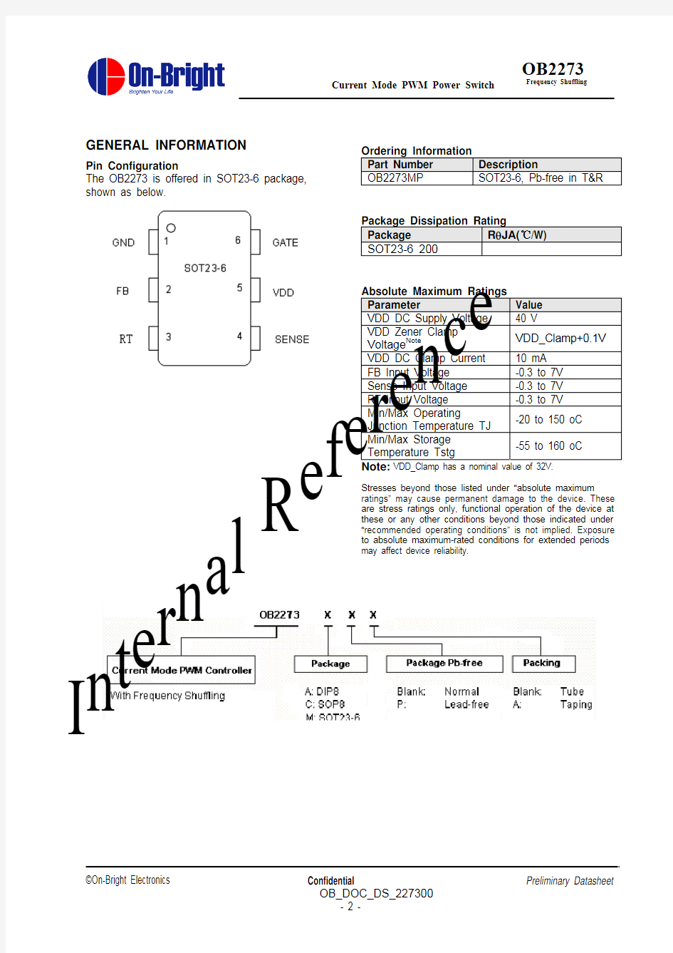
Pin Configuration
The OB2273 is offered in SOT23-6 package,
shown as below.
Ordering Information Part Number Description OB2273MP SOT23-6, Pb-free in T&R
Package Dissipation Rating Package R θJA(℃/W)
SOT23-6 200
Absolute Maximum Ratings Parameter Value VDD DC Supply Voltage 40 V VDD Zener Clamp
Voltage Note
VDD_Clamp+0.1V
VDD DC Clamp Current 10 mA FB Input Voltage -0.3 to 7V Sense Input Voltage -0.3 to 7V RT Input Voltage -0.3 to 7V Min/Max Operating
Junction Temperature TJ -20 to 150 oC
Min/Max Storage
Temperature Tstg
-55 to 160 oC
Note:VDD_Clamp has a nominal value of 32V.
Stresses beyond those listed under “absolute maximum ratings” may cause permanent damage to the device. These are stress ratings only, functional operation of the device at these or any other conditions beyond those indicated under “recommended operating conditions” is not implied. Exposure to absolute maximum-rated conditions for extended periods may affect device reliability.
I n
t e
r n a l R
e f
e r e
n c e
Marking Information
TERMINAL ASSIGNMENTS
For SOT23-6
Pin Name I/O Description GND P Ground
FB I
Feedback input pin. The PWM duty cycle is determined by voltage level into this pin
and the current-sense signal at Pin 3.
RT I Dual function pin. Either connected through a NTC resistor to ground for over
temperature shutdown/latch control or connected through Zener to VDD for
adjustable over voltage protection
CS I Current sense input VDD P Power
Supply Gate O Totem-pole gate driver output for power Mosfet
RECOMMENDED OPERATING CONDITION
Symbol Parameter
Min/Max Unit VDD VDD Supply Voltage
10 to 30 V T A
Operating Ambient Temperature
-20 to 85
℃
C: Optional Internal Code
I n
t e
r n a
l R
e f
e r
e
n c e
BLOCK DIAGRAM
I n
t e r n a
l R e f
e r e
n c e
ELECTRICAL CHARACTERISTICS
(T A = 25℃, VDD=16V, unless otherwise noted) Symbol Parameter Test Conditions Min Typ Max Unit
Supply Voltage (VDD) Istartup
VDD Start up Current
VDD=11V,Measure
Leakage current into VDD
5 20 uA I_VDD_Operation Operation Current
V FB =3V 1.8 2.5 mA UVLO(ON)
VDD Under Voltage Lockout
Enter
6 7 8 V
UVLO(OFF)
VDD Under Voltage Lockout
Exit (Recovery)
12.5 13.5 14.5V
Vpull-up Pull-up PMOS active 13 V Vdd_clamp
Ivdd =10mA 30 32 34 V OVP(ON) Over voltage protection
voltage
CS=0V,FB=3V
Ramp up VDD until gate clock is off
24 26 28 V
Vlatch_release Latch release voltage 5 V Feedback Input Section(FB Pin)
V FB_Open V FB Open Loop Voltage 3.9 4.2 V
Avcs PWM input gain ΔVFB/Δ
VCS
2 V/V
Maximum duty cycle Max duty cycle @
VDD=14V,VFB=3V,VCS=0V
75 80 85 %
Vref_green The threshold enter green
mode
1.4 V
Vref_burst_H The threshold exit burst
mode
0.675 V
Vref_burst_L The threshold enter burst
mode
0.575 V
I FB _Short FB pin short circuit current Short FB pin to GND
and measure current
0.3 mA
V TH _PL Power Limiting FB
Threshold Voltage
3.7 V
T D _PL Power limiting Debounce
Time
80 88 96 mSec
Z FB _IN Input Impedance 4 Kohm Current Sense Input(Sense Pin) Soft start time 4 ms T_blanking Leading edge blanking time 220 ns Z SENSE _IN Input Impedance 40 Kohm
T D _OC Over Current Detection and
Control Delay
From Over Current
Occurs till the Gatedrive output start to turn off
120
nSec V TH _OC Internal Current Limiting Threshold Voltage FB=3.3V
0.75 V
Vocp_clamper CS voltage clamper 0.9 V Oscillator
F OSC Normal Oscillation Frequency VDD =14V, FB =
3V,
CS=0V
60 65 70 KHZ
△f_OSC Frequency jittering +/-4 % F_shuffling Shuffling frequency 32 Hz
△f_Temp Frequency Temperature
Stability
1 %
I n
t e
r n a
l R
e f
e r e
n c e
△f_VDD Frequency Voltage Stability 1 % F_Burst Burst Mode Base
Frequency
22 KHZ
Gate driver VOL
Ouput low level @
VDD=14V, Io=5mA
1 V
VOH Ouput high level @
VDD=14V, Io=20mA
6 V
V_clamp Output clamp voltage 12 V
T_r Output rising time 1V ~ 12V
@ CL=1000pF
175 nS
T_f Output falling time 12V ~ 1V
@ CL=500pF
85 nS
Over temperature protection IRT Output current of RT pin 95 100 105uA VOTP Threshold voltage for OTP 0.95 1 1.05V Td_OTP OTP debounce time 32 Cycle VRT_FL Float voltage at RT pin 2.3 V
Vth_OVP External OVP threshold
voltage
4 V
I n
t e
r n a
l R
e f
e r e
n c e
CHARACTERIZATION PLOTS
VDD = 18V, TA = 25℃ condition applies if not otherwise noted.
OPERATION DESCRIPTION
The Briard is a low power off-line SMPS Switcher optimized for off-line flyback converter applications in 40W~60W power range. The ‘Extended burst mode’ control greatly reduces the standby power consumption and helps the design easily to meet the international power conservation requirements.
? Startup Current and Start up Control
Startup current of Briard is designed to be very low so that VDD could be charged up above UVLO threshold level and device starts up quickly. A large value startup resistor can therefore be used to minimize the power loss yet achieve a reliable startup in application. For AC/DC adapter with universal input range design, a 2 M ?, 1/8 W startup resistor could be used together with a VDD capacitor to provide a fast startup and yet low power dissipation design solution.
? Operating Current
The Operating current of Briard is low at 1.8mA. Good efficiency is achieved with Briard low operating current together with the ‘Extended burst mode’ control features.
? Soft Start
Briard features an internal 4ms soft start to soften the electrical stress occurring in the power supply during startup. It is activated during the power on sequence. As soon as VDD reaches UVLO(OFF), the CS peak voltage is gradually increased from 0.15V to the maximum level. Every restart up is followed by a soft start.
? Frequency shuffling for EMI improvement The frequency Shuffling (switching frequency modulation) is implemented in Briard. The oscillation frequency is modulated so that the tone energy is spread out. The spread spectrum minimizes the conduction band EMI and therefore eases the system design.
? Extended Burst Mode Operation
At light load or zero load condition, most of the power dissipation in a switching mode power supply is from switching loss on the MOSFET, the core loss of the transformer and the loss on the snubber circuit. The magnitude of power loss is in proportion to the switching frequency. Lower switching frequency leads to the reduction on the power loss and thus conserves the energy.
The switching frequency is internally adjusted at no load or light load condition. The switch frequency reduces at light/no load condition to improve the conversion efficiency. At light load or no load condition, the FB input drops below burst mode threshold level and device enters Burst Mode control. The Gate drive output switches only when VDD voltage drops below a preset level and FB input is active to output an on state. Otherwise the gate drive remains at off state to minimize the switching loss and reduces the standby power consumption to the greatest extend.
The switching frequency control also eliminates the audio noise at any loading conditions.
? Oscillator Operation
The switching frequency of Briard is internally fixed at 65KHZ. No external frequency setting components are required for PCB design simplification.
? Current Sensing and Leading Edge Blanking Cycle-by-Cycle current limiting is offered in Briard current mode PWM control. The switch current is detected by a sense resistor into the sense pin. An internal leading edge blanking circuit chops off the sensed voltage spike at initial internal power MOSFET on state due to snubber diode reverse recovery and surge gate current of power MOSFET so that the external RC filtering on sense input is no longer needed. The current limiting comparator is disabled and cannot turn off the internal power MOSFET during the blanking period. The PWM duty cycle is determined by the current sense input voltage and the FB input voltage.
? Internal Synchronized Slope Compensation Built-in slope compensation circuit adds voltage ramp onto the current sense input voltage for PWM generation. This greatly improves the close loop stability at CCM and prevents the sub-harmonic oscillation and thus reduces the output ripple voltage.
? Drive
The power MOSFET is driven by a dedicated gate driver for power switch control. Too weak the gate drive strength results in higher conduction and switch loss of MOSFET while too strong gate drive results the compromise of EMI.
A good tradeoff is achieved through the built-in totem pole gate design with right output strength
I n
t e
r n a
l R
e f
e r e
n c e
and dead time control. The low idle loss and good EMI system design is easier to achieve with this dedicated control scheme. ? Protection Controls
Good power supply system reliability is achieved with auto-recovery protection features including Cycle-by-Cycle current limiting (OCP), Over Load Protection (OLP), CS short protection, CS floating protection, and Under Voltage Lockout on VDD (UVLO), and latch features including over temperature protection (OTP), fixed or adjustable over voltage protection (OVP).
With On-Bright Proprietary technology, the OCP is line voltage compensated to achieve constant
output power limit over the universal input voltage range.
At overload condition when FB input voltage exceeds power limit threshold value for more than TD_PL, control circuit reacts to shut down the switcher. Switcher restarts when VDD voltage drops below UVLO limit. For latch mode, control circuit shutdowns (latch) the power MOSFET when an Over Temperature condition or Over Voltage condition is detected until VDD drops below 5V (Latch release voltage) , and device enters power on restart-up sequence thereafter .
I n
t e
r n a
l R
e f
e r e
n c e
PACKAGE MECHANICAL DATA
Dimensions In Millimeters Dimensions In Inches Symbol
Min Max Min Max
A 1.000 1.300 0.039 0.051 A1 0.000 0.150 0.000 0.006 A2 1.000 1.200 0.039 0.047 b 0.300 0.500 0.012 0.020 c 0.100 0.200 0.004 0.008 D 2.800 3.020 0.110 0.119 E 1.500 1.700 0.059 0.067 E1 2.600 3.000 0.102 0.118 e 0.950 (BSC) 0.037 (BSC)
e1 1.800 2.000 0.071 0.079 L 0.300 0.600 0.012 0.024 θ 0o 8o 0o 8o
I n
t e
r n a
l R
e f
e r e
n c e
IMPORTANT NOTICE
RIGHT TO MAKE CHANGES
On-Bright Electronics Corp. reserves the right to make corrections, modifications, enhancements, improvements and other changes to its products and services at any time and to discontinue any product or service without notice. Customers should obtain the latest relevant information before placing orders and should verify that such information is current and complete.
WARRANTY INFORMATION
On-Bright Electronics Corp. warrants performance of its hardware products to the specifications applicable at the time of sale in accordance with its standard warranty. Testing and other quality control techniques are used to the extent it deems necessary to support this warranty. Except where mandated by government requirements, testing of all parameters of each product is not necessarily performed.
On-Bright Electronics Corp. assumes no liability for application assistance or customer product design. Customers are responsible for their products and applications using On-Bright’s components, data sheet and application notes. To minimize the risks associated with customer products and applications, customers should provide adequate design and operating safeguards.
LIFE SUPPORT
On-Bright Electronics Corp.’s products are not designed to be used as components in devices intended to support or sustain human life. On-bright Electronics Corp. will not be held liable for any damages or claims resulting from the use of its products in medical applications.
MILITARY
On-Bright Electronics Corp.’s products are not designed for use in military applications. On-Bright Electronics Corp. will not be held liable for any damages or claims resulting from the use of its products in military applications.
I n
t e
r n a
l R
e f
e r e
n c e