TS612

s LOW NOISE:3nV/√Hz, 1.2pA/√Hz
s HIGH OUTPUT CURRENT:200mA
s VERY LOW HARMONIC AND INTERMODU-LATION DISTORTION
s HIGH SLEW RATE:40V/μs
s SPECIFIED FOR25?LOAD DESCRIPTION
The TS612is a dual operational amplifier featur-ing a high output current(200mA min.),large gain-bandwidth product(130MHz)and capable of driving a25?load with a160mA output current at ±6V power supply.
This device is particularly intended for applications where multiple carriers must be amplified simulta-neously with very low intermodulation products.
The TS612is housed in SO20batwing plastic package for a very low thermal resistance.It is also available in TSSOP14plastic package.This tiny package comes very interesting for surface saving.
The TS612is fitted out with Power Down function in order to decrease the consumption. APPLICATION
s UPSTREAM line driver for Asymmetric Digital Subscriber Line(ADSL)(NT).
ORDER CODE
D=Small Outline Package(SO)-also available in Tape&Reel(DT)
P=Thin Skrink Small Outline Package-only available in Tape&Reel(PT)PIN CONNECTIONS(top view)
Part Number Temperature
Range
Package
D P
TS612ID-40,+85°C?
TS612IPT-40,+85°C?
D
SO20Batwing
(Plastic Micropackage)
PT
TSSOP14
(Plastic Micropackage)
Vc c+1
Invertin ginput1
Non-invertinginput1
Vc c+2
Vc c-
Vc c-
Power Down2
Non-Invertinginput2
Invertinginput2
GND
Vc c-
Vc c-
Vc c-
Vc c-
Vc c-
Vc c-
Power Down1
Vc c-
Output1
Ou tpu t2
1
2
3
4
5
6
7
8
9
10
20
19
18
17
16
15
14
13
12
11
_
+
_
+
SO20ba twing-T o p Vie w
Therm alHea t Tabs
connectedto-V cc
Therm al Heat Tabs
connectedto-V cc
TS SOP14-T opView
Non-inv ertinginp ut2
Po wer Down2
No n-Inv ertinginp ut1
Inverting inp ut1
Vcc+1
Outpu t1
Vcc+2
NC
Vcc-
1
2
3
4
5
6
14
13
12
11
10
Invertinginput2
Output2
NC
Po werDow n1
9
8
7
_
+
GND
_
+
TS612
DUAL WIDE BAND OPERATIONAL AMPLIFIER
WITH HIGH OUTPUT CURRENT
TS612
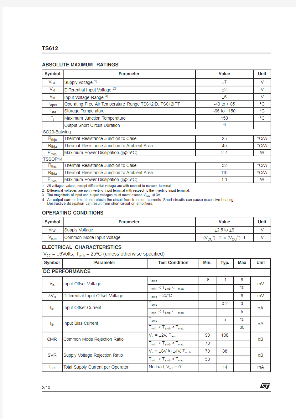
ABSOLUTE MAXIMUM RATINGS
OPERATING CONDITIONS
ELECTRICAL CHARACTERISTICS
V CC =±6Volts,T amb =25°C (unless otherwise specified)
Symbol Parameter
Value Unit V CC Supply voltage 1)
±7V V id Differential Input Voltage 2)±2V V in Input Voltage Range 3)
±6V T oper Operating Free Air Temperature Range TS612ID,TS612IPT -40to +85°C T std Storage Temperature
-65to +150
°C T j
Maximum Junction Temperature 150
°C
Output Short Circuit Duration
4)
SO20-Batwing R thjc Thermal Resistance Junction to Case 25°C/W R thja Thermal Resistance Junction to Ambient Area 45°C/W P max.
Maximum Power Dissipation (@25°C)
2.7W TSSOP14R thjc Thermal Resistance Junction to Case 32°C/W R thja Thermal Resistance Junction to Ambient Area 110°C/W P max.
Maximum Power Dissipation (@25°C)
1.1
W
1.All voltages values,except differential voltage are with respect to network terminal.
2.Differential voltages are non-inverting input terminal with respect to the inverting input terminal.
3.The magnitude of input and output voltages must never exceed V CC +0.3V.
4.An output current limitation protects the circuit from transient currents.Short-circuits can cause excessive heating.Destructive dissipation can result from short circuit on amplifiers.
Symbol Parameter
Value Unit V CC Supply Voltage
±2.5to ±6V V icm
Common Mode Input Voltage
(V CC -)+2to (V CC +)-1
V
Symbol
Parameter
Test Condition
Min.
Typ.
Max
Unit
DC PERFORMANCE
V io Input Offset Voltage
T amb
-6
-1
6mV T min. Input Offset Current T amb 0.2 3μA T min. 515μA T min. CMR Common Mode Rejection Ratio V ic =±2V,T amb 90108dB T min. I CC Total Supply Current per Operator No load,V out =0 14mA TS612 DYNAMIC PERFORMANCE and OUTPUT CHARACTERISTICS V OH High Level Output Voltage I out=160mA R L connected to GND 4 4.5V V OL Low Level Output Voltage I out=160mA R L connected to GND -4.5-4V A VD Large Signal Voltage Gain V out=7V peak R L=25?,T amb650011000V/V T min. GBP Gain Bandwidth Product A VCL=+11,f=20MHz R L=100? 80130MHz SR Slew Rate A VCL=+7,R L=50?2340V/μs I sink I source Output Short Circuit Current V id=±1V,T amb±200±320 mA T min. ΦM14Phase Margin at A VCL=14dB R L=25?//15pF60° ΦM6Phase Margin at A VCL=6dB R L=25?//15pF40°NOISE AND DISTORTION en Equivalent Input Noise Voltage f=100kHz3nV/√Hz in Equivalent Input Noise Current f=100kHz 1.2pA/√Hz THD Total Harmonic Distortion V out=4Vpp,f=100kHz A VCL=-10 R L=25?//15pF -69dB HD2-102nd Harmonic Distortion V out=4Vpp,f=100kHz A VCL=-10 Load=25?//15pF -70dBc HD2+22nd Harmonic Distortion V out=4Vpp,f=100kHz A VCL=+2 Load=25?//15pF -74dBc HD3+23rd Harmonic Distortion V out=4Vpp,f=1MHz A VCL=+2 Load=25?//15pF -79dBc HD3-103rd Harmonic Distortion V out=4Vpp,f=100kHz A VCL=-10 Load=25?//15pF -80dBc IM2-102nd Order Intermodulation Product F1=80kHz,F2=70kHz V out=8Vpp,A VCL=-10 Load=25?//15pF -77dBc IM3-103rd Order Intermodulation Product F1=80kHz,F2=70kHz V out=8Vpp,A VCL=-10 Load=25?//15pF -77dBc Symbol Parameter Test Condition Min.Typ.Max Unit TS612 POWER DOWN MODE V CC =±6Volts,T amb =25°C POWER DOWN EQUIVALENT SHEMATIC OUPUT IMPEDANCE IN POWER DOWN MODE In Power Down Mode the output of the driver is in ”high impedance”state.It is really the case for the static mode.Regarding the dynamic mode,the im-pedance decreases due to a capacitive effect of the collector-substrat and base collector junction.The impedance behaviour comes capacitive,typi-cally:1.4M ?//33pF. INTERMODULATION DISTORTION The curves shown below are the measurements results of a single operator wired as an adder with a gain of 15dB. The operational amplifier is supplied by a symmet-ric ±6V and is loaded with 25?. Two synthesizers (Rhode &Schwartz SME)gen-erate two frequencies (tones)(70&80kHz or 180&280kHz). An HP3585spectrum analyzer measures the spu-rious level at different frequencies. The curves are traced for different output levels (the value in the X ax is the value of each tone).The output levels of the two tones are the same.The generators and spectrum analyzer are phase locked to enhance measurement precision. 3rd ORDER INTERMODULATION (2tones :70kHz and 80kHz) 2nd ORDER INTERMODULATION Spurious measurement @100kHz (2tones :180kHz and 280kHz) 3rd ORDER INTERMODULATION (2tones :180kHz and 280kHz) Symbol Parameter Min. Typ. Max Unit V pdw Thershold Voltage for Power Down Mode V Low Level 00.8High Level 2 3.3Icc pdw Power Down Mode Current Consumption 75 μA R pdw Power Down Mode Ouput Impedance 1.4Μ?C pdw Power Down Mode Output Capacitance 33 pF STANDBY CONTROL OPERATOR STATUS pin (1)operator 1pin (7)operator 2operator 1operator 2V high level V low level Standby Active V high level V high level Standby Standby V low level V low level Active Active V low level V high level Active Standby +_.. ..V cc - V cc +POWER DOWN Ouput . 1 1,5 2 2,533,544,5 -100 -90 -80-70-60-50-40-30 -20-10 0I M 3(d B c ) Vout peak (V) 230kHz 220kHz 90kHz 60kHz Vout peak (V) 1,5 22,533,544,5 -70-65 -60 -55 I M 2(d B c ) 1 1,5 2 2,5 33,544,5 -100 -90-80-70-60-50-40-30 -20-100I M 3(d B c ) Vout peak (V) 80kHz 640kHz 380kHz 740kHz TS612 Closed Loop Gain and Phase vs.Frequency Gain=+2,Vcc=±6V,RL=25? Closed Loop Gain and Phase vs.Frequency Gain=+11,Vcc=±6V,RL=25? Maximum Output Swing Vcc=±6V,RL=25? Closed Loop Gain and Phase vs.Frequency Gain=+6,Vcc=±6V,RL=25? Equivalent Input Voltage Noise Gain=+100,Vcc=±6V,no load Channel Separation (Xtalk)vs.Frequency XTalk=20Log(V2/V1),Vcc=±6V,RL=25? -30-20-10 10G a i n (d B ) -200-1000 100200P h a s e (d e g r e e s ) 10kHz 100kHz 1MHz 10MHz 100MHz Frequ ency Gain Phase -30 -20-100 10 20 30G a i n (d B ) -200 -1000100 200 P h a s e (d e g r e e s ) 10kHz 100kHz 1MHz 10MHz 100MHz Frequen cy Gain Phase 2 46810 Time (μs)-5-4-3-2-1012 345s w i n g (V ) output input -20-15 -10-5 0510 15 20G a i n (d B ) -200 -100 100200 P h a s e (d e g r e e s ) 10kHz 100kHz 1MHz 10MHz 100MHz Frequ ency Gain Phase 100Hz 1kHz 10kHz 100kHz 1MHz 5 10 1520 e n (n V /V H z ) _ +100 10k Frequency -100 -90 -80-70-60-50-40-30 -20-10 X t a l k (d B ) 10kHz 100kHz 1MHz 10MHz Frequency 100? +_ 1k ? 49.9? V1 VIN 100? +_ 1k ? 49.9? V2 25? 25? ADSL CONCEPT Asymmetric Digital Subscriber Line (ADSL),is a new modem technology,which converts the exist-ing twisted-pair telephone lines into access paths for multimedia and high speed data communica-tions. ADSL transmits more than 8Mbps to a subscriber,and can reach 1Mbps from the subscriber to the central office.ADSL can literally transform the ac-tual public information network by bringing mov-ies,television,video catalogs,remote CD-ROMs,LANs,and the Internet into homes. An ADSL modem is connected to a twisted-pair telephone line,creating three information chan-nels:a high speed downstream channel (up to 1.1MHz)depending on the implementation of the ADSL architecture,a medium speed upstream channel (up to 130kHz)and a POTS (Plain Old Telephone Service),split off from the modem by filters. THE LINE INTERFACE -ADSL Remote Terminal (RT): The Figure1shows a typical analog line interface used for ADSL.The upstream and downstream signals are separated from the telephone line by using an hybrid circuit and a line transformer.On this note,the accent will be made on the emission path. The TS612is used as a dual line driver for the up-stream signal. For the remote terminal it is required to create an ADSL modem easy to plug in a PC.In such an ap-plication,the driver should be implemented with a +12volts single power supply.This +12V supply is available on PCI connector of purchase. The figure 2shows a single +12V supply circuit that uses the TS612as a remote terminal trans-mitter in differential mode. The driver is biased with a mid supply (nominaly +6V),in order to maintain the DC component of the signal at +6V.This allows the maximum dy-namic range between 0and +12V.Several op-tions are possible to provide this bias supply (such as a virtual ground using an operational amplifier),such as a two-resistance divider which is the cheapest solution.A high resistance value is re-quired to limit the current consumption.On the other hand,the current must be high enough to bias the inverting input of the TS612.If we consid-er this bias current (5μA)as the 1%of the current through the resistance divider (500μA)to keep a stable mid supply,two 47k ?resistances can be used. The input provides two high pass filters with a break frequency of about 1.6kHz which is neces-sary to remove the DC component of the input sig-nal.To avoid DC current flowing in the primary of the transformer,an output capacitor is used. Figure 1:Typical ADSL Line Interface impedance matching twisted-pair telephone line HYBRID CIRCUIT digital treatment LP filter TS612ID Line Driver reception (analog) emission (analog) digital to analog analogto digital high output current reception circuits upstream downstream Figure 2:TS612as a differential line driver with a +12V single supply R1 R3R2 Vi Vi Vo Vo GND +12V 25? 100? 1:2 Hybrid & Transformer GND +12V 47k 47k 10μ100n 100n 100n 1k 1k 12.5 12.5 10n 1μ +12V + _ +_ GND TYPICAL APPLICATION :TS612AS DRIVER FOR ADSL LINE INTERFACES A SINGLE SUPPLY IMPLEMENTATION WITH PASSIVE OR ACTIVE IMPEDANCE MATCHING by C.PRUGNE TS612 The 1μF capacitance provides a path for low fre-quencies,the 10nF capacitance provides a path for high end of the spectrum. In differential mode the TS612is able to deliver a typical amplitude signal of 18V peak to peak.The dynamic line impedance is 100?.The typical value of the amplitude signal required on the line is up to 12.4V peak to peak.By using a 1:2trans-former ratio the reflected impedance back to the primary will be a quarter (25?)and therefore the amplitude of the signal required with this imped-ance will be the half (6.2V peak to peak).Assum-ing the 25?series resistance (12.5?for both out-puts)necessary for impedance matching,the out-put signal amplitude required is 12.4V peak to peak.This value is acceptable for the TS612.In this case the load impedance is 25?for each driv-er. For the ADSL upstream path,a lowpass filter is absolutely necessary to cutoff the higher frequen-cies from the DAC analog output.In this simple non-inverting amplification configuration,it will be easy to implement a Sallen-Key lowpass filter by using the TS612.For ADSL over POTS,a maxi-mum frequency of 135kHz is reached.For ADSL over ISDN,the maximum frequency will be 276kHz. INCREASING THE LINE LEVEL BY USING AN ACTIVE IMPEDANCE MATCHING With passive matching,the output signal ampli-tude of the driver must be twice the amplitude on the load.To go beyond this limitation an active maching impedance can be used.With this tech-nique it is possible to keep good impedance matching with an amplitude on the load higher than the half of the ouput driver amplitude.This concept is shown in figure3for a differential https://www.wendangku.net/doc/553094959.html,ponent calculation: Let us consider the equivalent circuit for a single ended configuration,figure4. Let us consider the unloaded system.Assuming the currents through R1,R2and R3as respectively: As Vo °equals Vo without load,the gain in this case becomes : The gain,for the loaded system will be (1): As shown in figure5,this system is an ideal gener-ator with a synthesized impedance as the internal impedance of the system.From this,the output voltage becomes: with Ro the synthesized impedance and Iout the output current.On the other hand Vo can be ex-pressed as: By identification of both equations (2)and (3),the synthesized impedance is,with Rs1=Rs2=Rs: Figure 3:TS612as a differential line driver with an active impedance matching R1 R4R2Vi Vi Vo Vo 25?100? 1:2 Hybrid & Transformer GND +12V 47k 47k 10μ100n 100n 100n 1k 1k 12.5 12.5 10n 1μ R3R5 Vo ° Vo ° GND +12V +12V + _ +_ GND Figure 4:Single ended equivalent circuit 1/2R1 R2 R3 + _ Vi Vo Rs1 -1 Vo ° 1/2RL 2Vi R 1--------Vi Vo °–()R 2--------------------------and Vi Vo +()R 3 -----------------------,G Vo noload ()Vi ------------------------------12R 2R 1----------R 2 R 3 ------++1R 2 R 3 ------–----------------------------------==GL Vo withload ()Vi -----------------------------------12--12R 2R 1----------R 2 R 3------++1R 2R 3 ------–----------------------------------1(),==Vo ViG ()RoIout ()–=2() ,Vo Vi 12R 2R 1----------R 2R 3------++ 1R 2R 3------–----------------------------------------------Rs 1Iout 1R 2 R 3 ------–---------------------3(),–=Ro Rs 1R 2R 3 ------–----------------4(),= TS612 Figure 5:Equivalent schematic.Ro is the synthesized impedance Unlike the level Vo °required for a passive imped-ance,Vo °will be smaller than 2Vo in our case.Let us write Vo °=kVo with k the matching factor vary-ing between 1and 2.Assuming that the current through R3is negligeable,it comes the following resistance divider: After choosing the k factor,Rs will equal to 1/2RL(k-1). A good impedance matching assumes: From (4)and (5)it becomes: By fixing an arbitrary value for R2,(6)gives: Finally,the values of R2and R3allow us to extract R1from (1),and it comes: with GL the required gain. CAPABILITIES The table below shows the calculated compo-nents for different values of k.In this case R2=1000?and the gain=16dB.The last column displays the maximum amplitude level on the line regarding the TS612maximum output capabilities (18Vpp diff.)and a 1:2line transformer ratio. POWER CONSUMPTION IN COMMUNICATION Conditions: Passive impedance matching Transformer turns ratio:2Power Supply:12V Maximun level required on the line:12.4Vpp Maximum output level of the driver:12.4Vpp Crest factor:5.3(Vp/Vrms)Power Supply:12V The TS612power consumption during emission on 900and 4550meter twisted pair telephone lines:450mW GL (gain for the loaded system) GL is fixed for the application requirements GL=Vo/Vi=0.5(1+2R2/R1+R2/R3)/(1-R2/R3)R12R2/[2(1-R2/R3)GL-1-R2/R3]R2(=R4)Abritrary fixed R3(=R5)R2/(1-Rs/0.5RL)Rs 0.5RL(k-1) Ro Vi.Gi Iout 1/2RL Ro kVoRL RL 2Rs 1 +---------------------------=Ro 1 2 --RL 5() ,=R 2R 3------12Rs RL ---------6() ,–=R 3R 2 12Rs RL ---------–-------------------=R 12R 2 21R 2R 3------– GL 1–R 2R 3 ------–---------------------------------------------------------7() ,=Active matching k R1(?)R3(?) Rs (?) TS612Output Level to get 12.4Vpp on the line (Vpp diff) Maximum Line level (Vpp diff)1.38201500 3.9827.51.44901600 5.18.725.71.53602200 6.29.325.31.627024007.59.923.71.7 24033009.110.522.3Passive matching 12.4 18 TS612 PACKAGE MECHANICAL DATA 20PINS-PLASTIC MICROPACKAGE(SO) Dim. Millimeters Inches Min.Typ.Max.Min.Typ.Max. A 2.650.104 a10.10.30.0040.012 a2 2.450.096 b0.350.490.0140.019 b10.230.320.0090.013 C0.50.020 c145°(typ.) D12.613.00.4960.512 E1010.650.3940.419 e 1.270.050 e311.430.450 F7.47.60.2910.299 L0.5 1.270.0200.050 M0.750.030 S8°(max.) TS612 PACKAGE MECHANICAL DATA 14PINS -THIN SHRINK SMALL OUTLINE PACKAGE (TSSOP) https://www.wendangku.net/doc/553094959.html,limeters Inches Min.Typ. Max.Min.Typ. Max.A 1.200.05A10.050.150.010.006A20.80 1.00 1.050.0310.039 0.041b 0.190.300.0070.15c 0.090.200.0030.012D 4.90 5.00 5.100.1920.1960.20E 6.400.252E1 4.30 4.40 4.500.1690.1730.177e 0.650.025k 0°8°0°8°l 0.50 0.60 0.75 0.09 0.0236 0.030 c E 1 k L E e b D PIN 1IDENTIFICATION 1 7 814S E A T I N G P L A N E C a a a C 0,25mm .010inch GAGE PLANE L 1 A A2 A1Information furnished is believed to be accurate and reliable.However,STMicroelectronics assumes no responsibil ity for the consequences of use of such information nor for any infring ement of patents or other rights of third parties which may result from its use.No license is granted by implication or otherwise under any patent or patent rights of STMicroelectronics.Specifications mentioned in this publication are subject to change without notice.This publ ication supersedes and replaces all information previously supplied.STMicroelectronics products are not authorized for use as critical components in life support devices or systems withou t express written approval of STMicroelectronics. ?The ST logo is a registered trademark of STMicroelectronics ?2001STMicroelectronics -Printed in Italy -All Rights Reserved STMicroelectronics GROUP OF COMPANIES Australia -Brazil -China -Finland -France -Germany -Hong Kong -India -Italy -Japan -Malaysia -Malta -Morocco Singapore -Spain -Sweden -Switzerland -United Kingdom ?https://www.wendangku.net/doc/553094959.html,