MSM6585中文资料

GENERAL DESCRIPTION
The MSM6585 is an version-up product of the MSM5205 voice synthesis IC. Mainly improved points are improvement for the precision of an internal DA converter, a built-in low-pass filter, and expansion on the sampling frequency. The MSM6585 does not include a control circuit to drive an external memory similar to the MSM5205. Therefore, the MSM6585 can be connected with not only semiconductor memories, but other memory media (CD-ROM, etc.) by the control of CPU.
FEATURES
?4-bit ADPCM method
?Built-in 12-bit DA converter
?
Built-in low-pass filter (LPF) (–40dB/oct)?Sampling frequencies: 4k/8k/16k/32kHz
?Master clock frequency (ceramic oscillator) : 640kHz
?Voice data synthesis : Supported by voice analysis editing tools AR76-202 and AR203?Package options :
18-pin plastic DIP (DIP18-P-300-2.54) (Product name : MSM6585RS)
24-pin plastic SOP (SOP24-P-430-1.27-K) (Product name : MSM6585 GS-K)30-pin plastic SSOP (SSOP30-P-56-0.65-K) (Product name : MSM6585 GS-AK)
DIFFERENCES BETWEEN MSM6585 AND MSM5205
MSM6585MSM5205?Master clock frequency:640kHz
384kHz
?Sampling frequency:4k/8k/16k/32kHz 4k/6k/8kHz ?ADPCM bit length:4-bit 3-bit/4-bit ?DA Converter:12-bit
10-bit
?Low-pass filter:
Included (–40dB/oct)Not included ?Overflow preventing circuit:Included Not included ?Power supply voltage:
4.5 to
5.5V 3.0 to
6.0V ?Operating current consumption:10mA
4mA
?Operating temperature:–40 to +85°C –30 to +70°C
?D3 to D0 input timing
MSM6585
ADPCM Voice Synthesis IC
VCK (O)D3 - D0input timing ADPCM Data
E2D0011-27-43
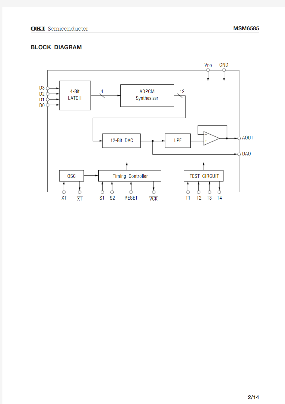
BLOCK DIAGRAM
D3
D2
D1
D0
AOUT
DAO XT XT S1S2RESET VCK T1T2T3T4
PIN CONFIGURATION (TOP VIEW)
18-Pin Plastic DIP S1S2T3D0D1D2D3T4GND V DD XT XT RESET VCK T2T1DAO AOUT
123456789
181716151413121110
S1S2
T3NC D0NC D1D2NC D3T4
GND V DD XT XT NC RESET NC VCK T2T1NC DAO AOUT
NC : No connection
24-Pin Plastic SOP
S1S2NC NC NC T3D0D1D2
D3NC NC V DD XT NC NC NC XT RESET VCK T2T1NC NC NC : No connection 30-Pin Plastic SSOP
NC T4GND NC DAO AOUT
PIN DESCRIPTION
Symbol Type
Description
S1
I
Pins to determine the sampling frequency.
The sampling frequencies of 32k, 16k, 8k, and 4kHz can be selected by combinations. (See the sampling frequencies in FUNCTIONAL DESCRIPTION on the selection of combinations.)
T3I Pin to test the internal circuit. Set this pin to a high level or make it open because it has a built-in pull-up resistor.D0-D3I Input pins for ADPCM data.
T4O Pin to test the internal circuit. Make this pin open.GND —Ground pin
AOUT O Pin to output the analog voice from the low-pass filter. Connect a 0.01 m F capacitor to this pin. (See the AOUT connecting circuit in FUNCTIONAL DESCRIPTION on the connecting circuit.)
DAO O Pin to output the analog voice from the DA converter.
T1I Pins to test the internal circuit. Set these pins to a low level or make them open because pull-down resistors are included.
VCK
O
This pin outputs the sampling frequency selected by the combinations of S1 and S2.
The voice synthesis starts or stops by synchronizing with VCK .RESET
I
Reset pin. The voice synthesis circuit is initialized by synchronizing with
VCK . If this pin is set to a high level, the D0 to D3 data inputs are disabled by synchronizing with VCK . The AOUT and DA0 pins output 1/2 V DD and become the state of no voice.
XT I Pin to connect an oscillator. When the external clock is used, input it from this pin.
XT O Pin to connect an oscillator.
When the external clock is used, make this pin open.
V DD
—
Power supply pin. Insert a bypass capacitor of 0.1 m F or more between this pin and the GND pin.
DIP SOP SSOP 111S22223364-75, 7,8, 107-108111491215101316111417121621T213172214
18
23
15
20
24
16222517232918
24
30
Pin Pin to test the internal circuit. Make this pin open.
ABSOLUTE MAXIMUM RATINGS
Condition Ta = 25°C Ta = 25°C —
Rating –0.3 to +7.0–0.3 to V DD +0.3–55 to +150
Unit V V °C
Symbol V DD V IN T STG
Parameter Power Supply Voltage Input Voltage Storage Temperature
(GND=0 V)
RECOMMENDED OPERATING CONDITIONS
ELECTRICAL CHARACTERISTICS
DC Characteristics
Min.0.8¥V DD –0.1V DD –0.4—20——–400–10–20——1050
Typ.————150——–120——5———
Max.V DD +0.10.2¥V DD —0.44001020–20——104040—
"H" Input Voltage Condition
Unit V V V V m A m A m A m A m A m A mA mV k W k W
Symbol
——
VCK: I OH = –40m A VCK: I OL = 40m A T1, T2, RESET: V IH = V DD S1, S2, D0 - D3, T3: V IH = V DD
XT: V IH = V DD T3: V IL = 0V S1, S2, D0 - D3, T1, T2,
RESET: V IL =0V
XT=V IL =0V f osc =640kHz, No load
No load ——
Parameter "L" Input Voltage "H" Output Voltage "L" Output Voltage "H" Input Current "H" Input Current "H" Input Current "L" Input Current "L" Input Current "L" Input Current Current Consumption DA Output Relative Error DA Output Impedance LPF Load Resistance
V IH V IL V OH V OL I IH1I IH2I IH3I IL1I IL2I IL3I DD | V DAE |R DAO R AOUT
(V DD =4.5 to 5.5V, GND=0V, Ta=–40 to +85°C)
Condition
Range Unit Symbol Parameter Power Supply Voltage Operating Temperature Master Clock Frequency
— 4.5 to 5.5V V DD —
–40 to +85°C T op oscillator connection
640
kHz
f OSC
(GND = 0V)
AC Characteristics
Min.Typ.Max.Parameter
Unit Symbol Condition
t VCK = 250m s
= 125m s = 62.5m s =31.25m s
f SAM = 4kHz ...
= 8kHz ... =16kHz ...=32kHz ...
Original Oscillation Duty Cycle
RESET Input Pulse Width Data Setup Time Data Hold Time
t W(RST)t S t H
f duty —
2¥t VCK —t VCK /2
———
—3—
m s m s m s
5060%40When data is shared with the MSM5205, note that the D3 to D0 selection timings of the MSM6585and MSM5205 are different. (Refer to DIFFERENCES BETWEEN MSM6585 AND MSM5205.)
TIMING DIAGRAM
The VCK clock rising and falling edges are reversed between the MSM5205 and the MSM6588, as indicated in DIFFERENCES BETWEEN MSM6585 AND MSM5205.
Note that the MSM6585 cannot accept data if the MSM5205 controls to repeat valid and invalid each half cycle, when the MSM5205 is replaced with the MSM6585.
VCK (O)
RESET (I)
D3 - D0 (I)
IC internalD3 - D0selection timings
AOUT, DAO (O)
FUNCTIONAL DESCRIPTION
1.
Sampling Frequency
The relationship of the sampling frequencies on S1 and S2, and the cutoff frequencies are listed below.
Cutoff frequency (f CUT )
1.6 kHz 3.2 kHz 6.4 kHz 1
2.8 kHz
Sampling frequency (f SAM )
4 kHz 8 kHz 16 kHz 32 kHz
S2L
L H
H
S1L H L H
2.AOUT Connecting Circuit
Connect a 0.01m F capacitor to the AOUT pin. The circuit diagram is as shown below.
Even when the DAO pin is used, connect a 0.01m F capacitor to the AOUT pin. This capacitor is used for the improvement of a voice quality.3.
Voice Output
The MSM6585 has two voice output pins. The DAO is direct output pin from the internal DA converter. The AOUT is a pin to output a voice after which the DAO output passed a built-in LPF.3.1
DA Converter Output Waveform
The output amplitude from the DA converter is max. (4095/4096) ¥ V DD and becomes a stair step waveform synchronized with the sampling frequency. The DAO output impedance varies in the ranges from 10k W to 40k W . Therefore, determine the filter constant so that the resistor variation does not have influence on the cutoff frequency of the filter.
3.2
Low-pass Filter Output
The cutoff frequency of the low-pass filter varies in proportion to the sampling frequency.The following figure shows the low-pass filter characteristics in the sampling frequency 8kHz.
4.Oscillation
Following show external circuit diagrams using a ceramic resonator, KBR-640B made by
Kyocera Corp. and CSB640P made by Murata MFG. Co., Ltd.
–20
–40
–60
1001k
10k
Frequency (Hz)
D a m p i n g f a c t o r (d B )
KBR-640B used
CSB640P used
APPLICATION CIRCUITS
Centronics Interface Circuit (sampling frequency : 8kHz)
BUSY STROBE RESET
D0D1D2D3D4D5D6D7
Centronics Timing Chart
RESET RES DATA STROBE
VCK KA KB BUSY
Example of Interface Circuit with 256K-bit EPROM
The circuit example and timing diagram that used the 256K-bit EPROM are shown below.
M6585 VCK (O)START SW M4013 S 1M4013 Q 1M4013 Q 2Q 2
M4040 Q 1
Q 2Q 12M4040 Q 3
Q 4
(M6585 RESET)
(Lower 4-bit)(Upper 4-bit)
PAD CONFIGURATION
Pad Layout
Product name MSM6585
Function ADPCM voice synthesis IC
Die size¥ = 2.92 mm, Y = 3.58 mm
Die thickness350 μm ±30 μm
Pad size130 μm ¥ 130 μm
Substrate voltage GND
Pad Coordiantes
(The die center is located at X=0, Y=0)
(Unit: m m) PAD No.PAD Name X-axis Y-axis PAD No.PAD Name X-axis Y-axis 1S1377–163511AOUT381635 2S2819–163512DAO–11251635 3T31305–163513T1–13051579 4D01305–94314T2–13051009 5D113054415VCK–1305–88 6D21305109516RESET–1305–818 7D31305163517XT–1281–1635 8T4830163518XT–529–1635 9AV SS447158019V DD–299–1549 10V SS267158020AV DD–119–1549
(Unit : mm) PACKAGE DIMENSIONS
DIP18-P-300-2.54
Package material Lead frame material Pin treatment Solder plate thickness Package weight (g)Epoxy resin 42 alloy Solder plating 5 m m or more 1.30 TYP.
(Unit : mm)
Notes for Mounting the Surface Mount Type Package
The SOP, QFP, TSOP, SOJ, QFJ (PLCC), SHP and BGA are surface mount type packages, which are very susceptible to heat in reflow mounting and humidity absorbed in storage.
Therefore, before you perform reflow mounting, contact Oki’s responsible sales person for the product name, package name, pin number, package code and desired mounting conditions (reflow method, temperature and times).
SOP24-P-430-1.27-K
Package material Lead frame material Pin treatment
Solder plate thickness Package weight (g)Epoxy resin 42 alloy
Solder plating 5 m m or more 0.58 TYP.
Mirror finish
(Unit : mm)
Notes for Mounting the Surface Mount Type Package
The SOP, QFP, TSOP, SOJ, QFJ (PLCC), SHP and BGA are surface mount type packages, which are very susceptible to heat in reflow mounting and humidity absorbed in storage.
Therefore, before you perform reflow mounting, contact Oki’s responsible sales person for the product name, package name, pin number, package code and desired mounting conditions (reflow method, temperature and times).
SSOP30-P-56-0.65-K
Package material Lead frame material Pin treatment
Solder plate thickness Package weight (g)Epoxy resin 42 alloy
Solder plating 5 m m or more 0.19 TYP.
Mirror finish