IVA-05228中文资料

Silicon Bipolar MMIC 1.5 GHz
Variable Gain Amplifier
Differential Option
Technical Data
IVA-05228
Features
? Differential Input and Output Capability
? DC to 1.5 GHz Bandwidth; 2.0 Gb/s Data Rates
? High Gain: 30 dB Typical
? Wide Gain Control Range:
30?dB Typical
? 5 V Bias
? 5 V V gc Control Voltage,
I gc
? Fast Gain Control Response: < 10 ns Typical
? Hermetic Ceramic Package Applications
? LNA or Gain Stage for 2.4?GHz and 5.7 GHz ISM Bands
? Front End Amplifier for GPS Receivers
? LNA or Gain Stage for PCN and MMDS Applications
? C-Band Satellite Receivers ? Broadband Amplifier for Instrumentation Description
The IVA-05228 is a variable gain
amplifier housed in a miniature
ceramic hermetic surface mount
package. This device can be used
in any combination of single-
ended or differential inputs or
outputs (see Functional Block
Diagram). The lowest frequency
of operation is limited only by the
values of user selected blocking
and bypass capacitors.
Typical applications include
variable gain amplification for
fiber optic systems (e.g., SONET)
with data rates up to 2.0 Gb/s,
mobile radio and satellite
receivers, millimeter wave
receiver IF amplifiers and
communication receivers.
The IVA series of variable gain
amplifiers is fabricated using HP’s
10 GHz f T, 25 GHz f MAX
ISOSAT?-I silicon bipolar
process. This process uses nitride
self-alignment, submicrometer
lithography, trench isolation, ion
implantation, gold metallization
and polyimide inter-metal
dielectric and scratch protection
to achieve excellent performance,
uniformity and reliability.
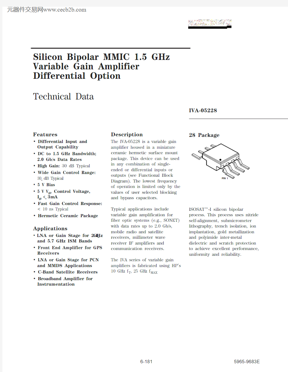
28 Package
Absolute Maximum Ratings
Notes:
1. The recommended operating voltage range for this device is 4 to 6 V. Typical performance as a function of voltage is on the following
page.
2. As measured using Input Pin 1 and Output Pin 6, with Output Pin 7 terminated into 50 ohms and Input Pin 4 at AC ground.
3. Referenced from 50 MHz Gain.
4. The recommended gain control range for these devices for dynamic control is 0 to 4.2 V. Operation at gain control settings above 4.2V
may result in gain increase rather than gain decrease.
IVA-05228 Typical Performance, T A = 25°C, V CC = 5 V, V ee = 0 V
G P (d B )
RF FREQUENCY (GHz)
TEMPERATURE (C)
Figure 3. Power Gain and P 1 dB at 0.5GHz and I CC vs. Case Temperature with V gc = 0 V.
–4–3–2–10
2530
35
40
45
–30–20–100
10
2030–55
+25+85
+125
–25V CC (V)
Figure 2. Power Gain and P 1 dB at 0.5GHz and I CC vs. Bias Voltage with V gc = 0 V.
Figure 1. Typical Variable Gain vs. Frequency.
I C C (
m A )
P 1 d B (d B m )
26
28303234G P (d B )
V gc (V)
Figure 4. Power Gain and P 1 dB at 0.5GHz and I gc
vs. Gain Control Voltage.
12
345
P 1 d B (d B m )
I g c (m A )
I C C (m A )
Typical Biasing Configuration and Functional Block Diagram
Differential Input/Differential Output
Single Ended Input/Single Ended Output
= 7 V
V ee V ee = 0 V
Input
Output –
Output +
Input
V ee Input
?*
* Optional: For Single-Ended Output operation, Pin 7 may be left unterminated (no C block or 50 ?)C bypass
= 1000 pF typical Good grounding of Pins 2, 3 is critical for proper operation and good VSWR performance of this part.
28 Package Outline
8 0.25 0.010)
DIMENSIONS ARE IN MILLIMETERS (INCHES)
V S W R
0.20.1
0.5 1.0 2.0 4.0
FREQUENCY (GHz)11.5
2
Figure 7. Input and Output VSWR vs. Frequency, V gc = 0–5 V.
t D (p s e c )
0.20.1
0.5 1.0 2.0 4.0
FREQUENCY (GHz)
300400
500
Figure 8. Group Delay vs. Frequency.
P 1 d B (d B m )
FREQUENCY (GHz)–25
–20
–15
–10
–5
Figure 5. P 1 dB vs. Frequency.
FREQUENCY (GHz)
Figure 6. Noise Figure vs. Frequency.
IVA-05228 Typical Performance, continued, T A = 25°C, V CC = 5 V, V ee = 0 V