RH1014MJ中文资料

1
Operational Amplifier
A U
G W A W
U
W A R BSOLUTE
XI TI S
The RH1014M is the first precision quad operational amplifier which directly upgrades designs in the industry standard 8-pin DIP LM124/LM148/OP-11/5156 pin con-figuration. Low offset voltage (300μV max), low drift (≤2.5μV/°C), low offset current (≤1.5nA), and high gain (1.2 million min) combine to make the RH1014M four truly precision amplifers in one package.
The wafer lots are processed to Linear Technology’s in-house Class S flow to yield circuits usable in stringent military applications.
D U
ESCRIPTIO
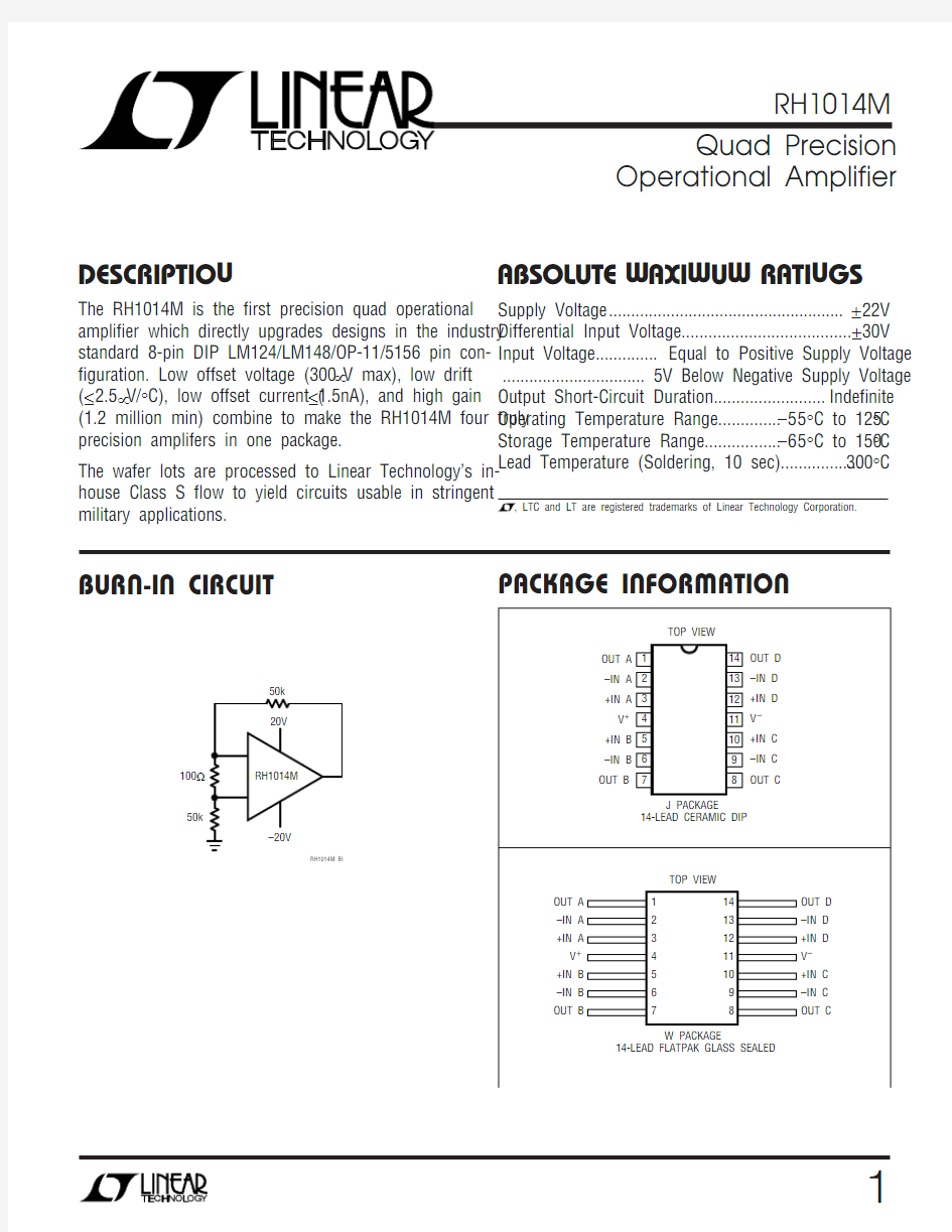
Supply Voltage (22)
Differential Input Voltage...................................... ±30V Input Voltage .............. Equal to Positive Supply Voltage ................................ 5V Below Negative Supply Voltage Output Short-Circuit Duration......................... Indefinite Operating Temperature Range..............–55°C to 125°C Storage Temperature Range.................–65°C to 150°
C Lead Temperature (Soldering, 10 sec)..................300°C
100RH1014M BI
BURN-IN CIRCUIT PACKAGE INFORMATION
2(Pre-Irradiation)
–55°C ≤ T A≤ 125°C
V S = ±15V, V CM = 0V, unless otherwise noted.
T A = 25°C SUB-SUB-SYMBOL PARAMETER CONDITIONS NOTES MIN TYP MAX GROUP MIN TYP MAX GROUP UNITS V OS Input Offset Voltage30015502,3μV
245017503μV
V CM = 0.1V, T A = 125°C27502μV ?V OS Average Tempco of Offset1 2.5μV/°C ?Temp Voltage
?V OS Long Term V OS Stability0.5μV/Mo ?Time
I OS Input Offset Current101202,3nA
2101202,3nA I B Input Bias Current301452,3nA
25011202,3nA e n Input Noise Voltage0.1Hz to 10Hz0.55μV P-P
Input Noise Voltage f O = 10Hz24nV/√Hz Density f O = 1000Hz22nV/√Hz i n Input Noise Current f O = 10Hz0.07pA/√Hz
Density
R IN Input Resistance Differential170M?
Common Mode4G?A VOL Large-Signal Voltage Gain V O = ±10V, R L≥ 2k 1.240.255,6V/μV
V O = ±10V, R L≥ 600?0.54V/μV
V O = 5mV to 4V, R L = 500?21V/μV Input Voltage Range1 13.5V
1–15.0V
1,2 3.5V
1,2 0V CMRR Common-Mode Rejection V CM = 13.5V, –15V971dB Ratio V CM = 13V, –14.9V942,3dB PSRR Power Supply Rejection V S = ±2V to ±18V1001972,3dB Ratio
Channel Separation V O = ±10V, R L = 2k1201dB V OUT Output Voltage Swing R L≥ 2k±12.54±11.55,6V
Output Low, No Load2254mV
Output Low, 600? to GND2104185,6mV
Output Low, I SINK = 1mA23504mV
Output High, No Load2 4.04V
Output High, 600? to GND2 3.44 3.15,6V SR Slew Rate0.24V/μs
I S Supply Current Per Amplifier0.5510.702,3mA
20.5010.652,3mA TABLE 1: ELECTRICAL CHARACTERISTICS
3
SYMBOL PARAMETER CONDITIONS
NOTES MIN MAX MIN MAX MIN MAX
MIN MAX
MIN MAX UNITS
V OS Input Offset Voltage
450450600750900
μV 2
600600750900μV I OS Input Offset Current
1010152025
nA 2
10101520nA I B
Input Bias Current
6075100175250nA 2
80
100
125
200
nA Input Voltage Range
1 13.5 13.5 13.5 13.5 13.5V 1–15.0–15.0–15.0–15.0–15.0
V 2 3.5 3.5 3.5 3.5V 2
0000V CMRR Common-Mode Rejection
V CM = 13V, –15V 9797949086dB Ratio
PSRR Power Supply Rejection V S = ±10V to ±18V 10098948680dB Ratio
A VOL Large-Signal Voltage Gain R L ≥ 10k, V O = ±10V 5002001005025V/mV
V OUT
Maximum Output Voltage R L ≥ 10k
±12.5
±12.5
±12.5
±12.5
±12.5
V Swing
Output Low, No Load 225304050mV Output Low, 600? to
GND 210101010mV Output Low, I SINK = 1mA 20.6
0.8
1.0
1.6
V Output High, No Load 2 4.0 4.0 4.0 4.0V Output High, 600? to GND
2
3.4 3.2 3.0 2.8V SR Slew Rate R L ≥ 10k 0.13
0.12
0.11
0.07
0.01
V/μs I S
Supply Current
Per Amplifier
0.550.550.550.550.55
mA 20.50
0.50
0.50
0.50
mA
V S = ±15V, V CM = 0V, T A = 25°C, unless otherwise noted.
TABLE 1A: ELECTRICAL CHARACTERISTICS (Post-Irradiation)
200KRAD(Si)
100KRAD(Si)
50KRAD(Si)
20KRAD(Si)10KRAD(Si)Note 1: Guaranteed by design, characterization, or correlation to other
tested parameters.
Note 2: Specification applies for V S + = 5V, V S – = 0V, V CM = 0V,V OUT = 1.4V.
4
MIL-STD-883 TEST REQUIREMENTS
SUBGROUP Final Electrical Test Requirements (Method 5004)1*,2,3,4,5,6Group A Test Requirements (Method 5005)1,2,3,4,5,6Group B and D for Class S
1,2,3
End Point Electrical Parameters (Method 5005)* PDA applies to subgroup 1. See PDA Test Notes.
TABLE 2: ELECTRICAL TEST REQUIRE E TS
U W
PDA Test Notes
The PDA is specified as 5% based on failures from group A, subgroup 1,tests after cooldown as the final electrical test in accordance with method 5004 of MIL-STD-883. The verified failures of group A, subgroup 1, after burn-in divided by the total number of devices submitted for burn-in in that lot shall be used to determine the percent for the lot.
Linear Technology Corporation reserves the right to test to tighter limits than those given.
TOTAL DOSE BIAS CIRCUIT
Negative Slew Rate
Positive Slew Rate
C C HARA TERISTICS
U W
A TYPICAL PERFOR CE TOTAL DOSE KRAD (Si)
1
N E G A T I V E S L E W R A T E (
V /μs )
0.8
0.6
0.4
0.2
101001000
RH1014M G03
TOTAL DOSE KRAD (Si)
1
P O S I T I V E S L E W R A T E (
V /μs )
0.8
0.6
0.4
0.2
101001000
RH1014M G02
TOTAL DOSE KRAD (Si)
1
S U P P L Y C U R R E N T
(m A )
0.8
0.6
0.40.20
101001000
RH1014M G01
Supply Current (Per Amplifier)
8V
5
C C HARA TERISTICS
U W
A TYPICAL PERFOR CE Power Supply Rejection Ratio
TOTAL DOSE KRAD (Si)
1
P O W E R S U P P L Y R E J E C T I O N R A T I O (d B )
140
130120110100908070
101001000
RH1014M G09
TOTAL DOSE KRAD (Si)
1
I N P U T N O I S E V O L T A G E D E N S I T Y (n V /√H z )
100
9080706050403020100101001000
RH1014M G10
Input Noise Voltage Density
TOTAL DOSE KRAD (Si)
1
G A I N B A N D W I D T H P R O D U C T (k H z )
1000
9008007006005004003002001000101001000
RH1014M G11
Gain Bandwidth Product
Open-Loop Gain
TOTAL DOSE KRAD (Si)
1
O P E N -L O O P G A I N (d B )
150
140
1301201101009080
101001000RH1014M G07
TOTAL DOSE KRAD (Si)
1
I N P U T O F F S E T V O L T A G E (μV )
3002001000
–100–200–300
101001000
RH1014M G04
Input Offset Voltage
Input Offset Current
TOTAL DOSE KRAD (Si)
1
I N P U T O F F S E T C U R R E N T (n A )
3
2
1
–1
–2
101001000
RH1014M G06
Input Bias Current
TOTAL DOSE KRAD (Si)
1
I N P U T B I A S C U R R E N T (n A )
7060
50403020100
101001000
RH1014M G05
TOTAL DOSE KRAD (Si)
1
C O M M O N -M O
D
E R E J E C T I O N R A T I O (d B )
1501401301201101009080
101001000
RH1014M G08
Common-Mode Rejection Ratio
I nformation furnished by Linear Technology Corporation is believed to be accurate and reliable.However, no responsibility is assumed for its use. Linear Technology Corporation makes no represen-tation that the interconnection of its circuits as described herein will not infringe on existing patent rights.
6
? I.D. No. 66-11-1014 Rev. G 1007
Linear Technology Corporation 1630 McCarthy Blvd., Milpitas, CA 95035-7417 (408) 432-1900 ● FAX: (408) 434-0507 ● https://www.wendangku.net/doc/6215728527.html,