sn74hc245

3212019910111213456781817161514B1B2B3B4B5
A3A4A5A6A7A 2A 1D I R B 7B 6O E A 8G N D B 8V C C (TOP VIEW)
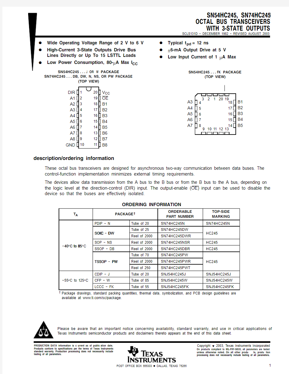
1234567891020191817161514131211DIR
A1
A2
A3
A4
A5
A6
A7
A8
GND V CC OE B1B2B3B4B5B6B7B8SN74HC245...DB, DW, N, NS, OR PW PACKAGE (TOP VIEW)description/ordering information
These octal bus transceivers are designed for asynchronous two-way communication between data buses. The
control-function implementation minimizes external timing requirements.
The devices allow data transmission from the A bus to the B bus or from the B bus to the A bus, depending on
the logic level at the direction-control (DIR) input. The output-enable (OE) input can be used to disable the
device so that the buses are effectively isolated.
ORDERING INFORMATION
T A
PACKAGE ?ORDERABLE PART NUMBER TOP-SIDE MARKING PDIP ? N
Tube of 20SN74HC245N SN74HC245N SOIC DW Tube of 25SN74HC245DW SOIC ? DW
Reel of 2000SN74HC245DWR HC24540°C to 85°C SOP ? NS
Reel of 2000SN74HC245NSR HC245?40C to 85SSOP ? DB
Reel of 2000SN74HC245DBR HC245Tube of 70SN74HC245PW TSSOP ? PW Reel of 2000SN74HC245PWR TSSOP PW
Reel of 250SN74HC245PWT HC245CDIP ? J
Tube of 20SNJ54HC245J SNJ54HC245J ?55°C to 125°C
CFP ? W Tube of 85SNJ54HC245W SNJ54HC245W LCCC ? FK Tube of 55SNJ54HC245FK SNJ54HC245FK ?Package drawings, standard packing quantities, thermal data, symbolization, and PCB design guidelines are
available at https://www.wendangku.net/doc/6616076341.html,/sc/package.
Please be aware that an important notice concerning availability, standard warranty, and use in critical applications of
Texas Instruments semiconductor products and disclaimers thereto appears at the end of this data sheet.
Copyright ? 2003, Texas Instruments Incorporated PRODUCTION DATA information is c urrent as of public ation date.
SN54HC245, SN74HC245OCTAL BUS TRANSCEIVERS WITH 3-STATE OUTPUTS SCLS131D ? DECEMBER 1982 ? REVISED AUGUST 2003FUNCTION TABLE
INPUTS
OE
DIR OPERATION L
L B data to A bus L
H A data to B bus H X Isolation
logic diagram (positive logic)
DIR OE
A1B1
To Seven Other Channels
absolute maximum ratings over operating free-air temperature range (unless otherwise noted)?
Supply voltage range, V CC ?0.5 V to 7 V
. . . . . . . . . . . . . . . . . . . . . . . . . . . . . . . . . . . . . . . . . . . . . . . . . . . . . . . . . . Input clamp current, I IK (V I < 0 or V I > V CC ) (see Note 1) ±20 mA
. . . . . . . . . . . . . . . . . . . . . . . . . . . . . . . . . . . . . Output clamp current, I OK (V O < 0 or V O > V CC ) (see Note 1) ±20 mA
. . . . . . . . . . . . . . . . . . . . . . . . . . . . . . . . . Continuous output current, I O (V O = 0 to V CC ) ±35 mA
. . . . . . . . . . . . . . . . . . . . . . . . . . . . . . . . . . . . . . . . . . . . . . Continuous current through V CC or GND ±70 mA
. . . . . . . . . . . . . . . . . . . . . . . . . . . . . . . . . . . . . . . . . . . . . . . . . . . Package thermal impedance, θJA (see Note 2):DB package 70°C/W
. . . . . . . . . . . . . . . . . . . . . . . . . . . . . . . . . DW package 58°C/W
. . . . . . . . . . . . . . . . . . . . . . . . . . . . . . . . . N package 69°C/W
. . . . . . . . . . . . . . . . . . . . . . . . . . . . . . . . . . . NS package 60°C/W
. . . . . . . . . . . . . . . . . . . . . . . . . . . . . . . . . PW package 83°C/W
. . . . . . . . . . . . . . . . . . . . . . . . . . . . . . . . . Storage temperature range, T stg ?65°C to 150°C
. . . . . . . . . . . . . . . . . . . . . . . . . . . . . . . . . . . . . . . . . . . . . . . . . . . ?
Stresses beyond those listed under “absolute maximum ratings” may cause permanent damage to the device. These are stress ratings only, and
functional operation of the device at these or any other conditions beyond those indicated under “recommended operating conditions” is not
implied. Exposure to absolute-maximum-rated conditions for extended periods may affect device reliability.
NOTES: 1.The input and output voltage ratings may be exceeded if the input and output current ratings are observed.
2.The package thermal impedance is calculated in accordance with JESD 51-7.
SN54HC245, SN74HC245OCTAL BUS TRANSCEIVERS WITH 3-STATE OUTPUTS SCLS131D ? DECEMBER 1982 ? REVISED AUGUST 2003recommended operating conditions (see Note 3)SN54HC245
SN74HC245MIN
NOM MAX MIN NOM MAX UNIT V CC
Supply voltage 256256V
V CC = 2 V 1.5 1.5High-level input voltage V CC = 4.5 V
3.15 3.15V IH High level input voltage V CC = 6 V
4.2 4.2V V CC = 2 V
0.50.5Low-level input voltage V CC = 4.5 V 1.35 1.35V IL
Low level input voltage V CC = 6 V 1.8 1.8V V I
Input voltage 0V CC 0V CC V V O
Output voltage 0V CC 0V CC V V CC = 2 V 10001000V CC = 4.5 V 500500Δt/Δv
Input transition rise/fall time V CC = 6 V 400400ns T A Operating free-air temperature ?55125?4085°C NOTE 3:All unused inputs of the device must be held at V CC or GND to ensure proper device operation. Refer to the TI application report,
Implications of Slow or Floating CMOS Inputs , literature number SCBA004.
electrical characteristics over recommended operating free-air temperature range (unless otherwise noted)TEST CONDITIONS T A = 25°C SN54HC245SN74HC245PARAMETER TEST CONDITIONS V CC
MIN TYP MAX MIN MAX MIN MAX UNIT
2 V
1.9 1.998 1.9 1.9 = ?20 4.5 V 4.4 4.499 4.4 4.4 = V I OH 20 μA
6 V 5.9 5.999 5.9 5.9V OH V I V IH or V IL
I OH = ?6 mA
4.5 V 3.98 4.3 3.7 3.84V I OH = ?7.8 mA
6 V 5.48 5.8 5.2 5.342 V 0.0020.10.10.1 = 20 μA
4.5 V 0.0010.10.10.1 = V I OL 20 6 V 0.0010.10.10.1V OL V I V IH or V IL
I OL = 6 mA
4.5 V 0.170.260.40.33V I OL = 7.8 mA
6 V 0.150.260.40.33I I
DIR or OE V I = V CC or 0 6 V ±0.1±100±1000±1000nA I OZ
A or
B V O = V C
C or 0 6 V ±0.01±0.5±10±5μA I CC
V I = V CC or 0,I O = 0 6 V 816080μA C i DIR or OE 2 V to 6 V 3101010pF
SN54HC245, SN74HC245
OCTAL BUS TRANSCEIVERS
WITH 3-STATE OUTPUTS
SCLS131D ? DECEMBER 1982 ? REVISED AUGUST 2003
switching characteristics over recommended operating free-air temperature range, C L = 50 pF (unless otherwise noted) (see Figure 1)
FROM TO T A = 25°C SN54HC245SN74HC245 PARAMETER(INPUT)(OUTPUT)V CC
UNIT
MIN TYP MAX MIN MAX MIN MAX
2 V40105160130
4.5 V15213226
ns t pd A or B B or A
6 V12182722
2 V125230340290
4.5 V23466858
ns t en OE A or B
6 V20395849
2 V74200300250
4.5 V25406050
t dis OE A or B
ns
6 V21345143
2 V20609075
t A or B 4.5 V8121815ns t
6 V6101513
switching characteristics over recommended operating free-air temperature range, C L = 150 pF (unless otherwise noted) (see Figure 1)
FROM TO T A = 25°C SN54HC245SN74HC245
UNIT PARAMETER(INPUT)(OUTPUT)V CC
MIN TYP MAX MIN MAX MIN MAX
2 V54135200170
4.5 V18274034
ns t pd A or B B or A
6 V15233429
2 V150270405335
4.5 V31548167
ns t en OE A or B
6 V25466956
2 V45210315265
t A or B 4.5 V17426353ns t
6 V13365345 operating characteristics, T A = 25°C
PARAMETER TEST CONDITIONS TYP UNIT
C pd Power dissipation capacitance per transceiver No load40pF
SN54HC245, SN74HC245OCTAL BUS TRANSCEIVERS WITH 3-STATE OUTPUTS SCLS131D ? DECEMBER 1982 ? REVISED AUGUST 2003PARAMETER MEASUREMENT INFORMATION
VOLTAGE WAVEFORM
INPUT RISE AND FALL TIMES
V CC 0 V Input VOLTAGE WAVEFORMS PROPAGATION DELAY AND OUTPUT TRANSITION TIMES
CC
OH OL OH OL
CC
VOLTAGE WAVEFORMS ENABLE AND DISABLE TIMES FOR 3-STATE OUTPUTS
From Output Under Test V CC
LOAD CIRCUIT
PARAMETER C L t PZH t pd or t t
t dis t en t PZL
t PHZ
t PLZ 1 k Ω1 k Ω50 pF or 150 pF 50 pF
Open Closed R L S1Closed Open S2Open Closed Closed Open 50 pF
or
150 pF Open Open ??NOTES: A.C L includes probe and test-fixture capacitance.
B.Waveform 1 is for an output with internal conditions such that the output is low except when disabled by the output control.
Waveform 2 is for an output with internal conditions such that the output is high except when disabled by the output control.
C.Phase relationships between waveforms were chosen arbitrarily. All input pulses are supplied by generators having the following
characteristics: PRR ≤ 1 MHz, Z O = 50 Ω, t r = 6 ns, t f = 6 ns.
D.The outputs are measured one at a time with one input transition per measurement.
E.t PLZ and t PHZ are the same as t dis .
F.t PZL and t PZH are the same as t en .
G.t PLH and t PHL are the same as t pd .
Figure 1. Load Circuit and Voltage Waveforms
PACKAGING INFORMATION
Orderable Device Status (1)Package Type Package
Drawing Pins Package Qty Eco Plan (2)Lead/
Ball Finish
MSL Peak Temp (3)Samples
(Requires Login)
5962-8408501VRA ACTIVE CDIP J201TBD A42N / A for Pkg Type Purchase Samples 5962-8408501VSA ACTIVE CFP W201TBD Call TI N / A for Pkg Type Purchase Samples 84085012A ACTIVE LCCC FK201TBD POST-PLATE N / A for Pkg Type Purchase Samples 8408501RA ACTIVE CDIP J201TBD A42N / A for Pkg Type Purchase Samples 8408501SA ACTIVE CFP W201TBD Call TI N / A for Pkg Type Purchase Samples JM38510/65503BRA ACTIVE CDIP J201TBD A42N / A for Pkg Type Contact TI Distributor
or Sales Office JM38510/65503BSA ACTIVE CFP W201TBD Call TI N / A for Pkg Type Contact TI Distributor
or Sales Office SN54HC245J ACTIVE CDIP J201TBD A42N / A for Pkg Type Contact TI Distributor
or Sales Office SN74HC245DBLE OBSOLETE SSOP DB20TBD Call TI Call TI Replaced by
SN74HC245DBR
SN74HC245DBR ACTIVE SSOP DB202000Green (RoHS
& no Sb/Br)CU NIPDAU Level-1-260C-UNLIM Contact TI Distributor
or Sales Office
SN74HC245DBRE4ACTIVE SSOP DB202000Green (RoHS
& no Sb/Br)CU NIPDAU Level-1-260C-UNLIM Contact TI Distributor
or Sales Office
SN74HC245DBRG4ACTIVE SSOP DB202000Green (RoHS
& no Sb/Br)CU NIPDAU Level-1-260C-UNLIM Contact TI Distributor
or Sales Office
SN74HC245DW ACTIVE SOIC DW2025Green (RoHS
& no Sb/Br)
CU NIPDAU Level-1-260C-UNLIM Purchase Samples
SN74HC245DWE4ACTIVE SOIC DW2025Green (RoHS
& no Sb/Br)
CU NIPDAU Level-1-260C-UNLIM Purchase Samples
SN74HC245DWG4ACTIVE SOIC DW2025Green (RoHS
& no Sb/Br)
CU NIPDAU Level-1-260C-UNLIM Purchase Samples
SN74HC245DWR ACTIVE SOIC DW202000Green (RoHS
& no Sb/Br)CU NIPDAU Level-1-260C-UNLIM Contact TI Distributor
or Sales Office
SN74HC245DWRE4ACTIVE SOIC DW202000Green (RoHS
& no Sb/Br)CU NIPDAU Level-1-260C-UNLIM Contact TI Distributor
or Sales Office
SN74HC245DWRG4ACTIVE SOIC DW202000Green (RoHS
& no Sb/Br)CU NIPDAU Level-1-260C-UNLIM Contact TI Distributor
or Sales Office
SN74HC245N ACTIVE PDIP N2020Pb-Free (RoHS)CU NIPDAU N / A for Pkg Type Contact TI Distributor
or Sales Office
Addendum-Page 1
Orderable Device Status (1)Package Type Package
Drawing Pins Package Qty Eco Plan (2)Lead/
Ball Finish
MSL Peak Temp (3)Samples
(Requires Login)
SN74HC245N3OBSOLETE PDIP N20TBD Call TI Call TI Samples Not Available SN74HC245NE4ACTIVE PDIP N2020Pb-Free (RoHS)CU NIPDAU N / A for Pkg Type Contact TI Distributor
or Sales Office
SN74HC245NSR ACTIVE SO NS202000Green (RoHS
& no Sb/Br)CU NIPDAU Level-1-260C-UNLIM Contact TI Distributor
or Sales Office
SN74HC245NSRE4ACTIVE SO NS202000Green (RoHS
& no Sb/Br)CU NIPDAU Level-1-260C-UNLIM Contact TI Distributor
or Sales Office
SN74HC245NSRG4ACTIVE SO NS202000Green (RoHS
& no Sb/Br)CU NIPDAU Level-1-260C-UNLIM Contact TI Distributor
or Sales Office
SN74HC245PW ACTIVE TSSOP PW2070Green (RoHS
& no Sb/Br)
CU NIPDAU Level-1-260C-UNLIM Purchase Samples
SN74HC245PWE4ACTIVE TSSOP PW2070Green (RoHS
& no Sb/Br)
CU NIPDAU Level-1-260C-UNLIM Purchase Samples
SN74HC245PWG4ACTIVE TSSOP PW2070Green (RoHS
& no Sb/Br)
CU NIPDAU Level-1-260C-UNLIM Purchase Samples
SN74HC245PWLE OBSOLETE TSSOP PW20TBD Call TI Call TI Replaced by
SN74HC245PWR
SN74HC245PWR ACTIVE TSSOP PW202000Green (RoHS
& no Sb/Br)CU NIPDAU Level-1-260C-UNLIM Contact TI Distributor
or Sales Office
SN74HC245PWRE4ACTIVE TSSOP PW202000Green (RoHS
& no Sb/Br)CU NIPDAU Level-1-260C-UNLIM Contact TI Distributor
or Sales Office
SN74HC245PWRG3PREVIEW TSSOP PW202000TBD Call TI Call TI Samples Not Available
SN74HC245PWRG4ACTIVE TSSOP PW202000Green (RoHS
& no Sb/Br)CU NIPDAU Level-1-260C-UNLIM Contact TI Distributor
or Sales Office
SN74HC245PWT ACTIVE TSSOP PW20250Green (RoHS
& no Sb/Br)
CU NIPDAU Level-1-260C-UNLIM Purchase Samples
SN74HC245PWTE4ACTIVE TSSOP PW20250Green (RoHS
& no Sb/Br)
CU NIPDAU Level-1-260C-UNLIM Purchase Samples
SN74HC245PWTG4ACTIVE TSSOP PW20250Green (RoHS
& no Sb/Br)
CU NIPDAU Level-1-260C-UNLIM Purchase Samples
SNJ54HC245FK ACTIVE LCCC FK201TBD POST-PLATE N / A for Pkg Type Contact TI Distributor
or Sales Office SNJ54HC245J ACTIVE CDIP J201TBD A42N / A for Pkg Type Contact TI Distributor
or Sales Office SNJ54HC245W ACTIVE CFP W201TBD Call TI N / A for Pkg Type Contact TI Distributor
or Sales Office
Addendum-Page 2
(1) The marketing status values are defined as follows:
ACTIVE: Product device recommended for new designs.
LIFEBUY: TI has announced that the device will be discontinued, and a lifetime-buy period is in effect.
NRND: Not recommended for new designs. Device is in production to support existing customers, but TI does not recommend using this part in a new design.
PREVIEW: Device has been announced but is not in production. Samples may or may not be available.
OBSOLETE: TI has discontinued the production of the device.
(2) Eco Plan - The planned eco-friendly classification: Pb-Free (RoHS), Pb-Free (RoHS Exempt), or Green (RoHS & no Sb/Br) - please check https://www.wendangku.net/doc/6616076341.html,/productcontent for the latest availability information and additional product content details.
TBD: The Pb-Free/Green conversion plan has not been defined.
Pb-Free (RoHS): TI's terms "Lead-Free" or "Pb-Free" mean semiconductor products that are compatible with the current RoHS requirements for all 6 substances, including the requirement that lead not exceed 0.1% by weight in homogeneous materials. Where designed to be soldered at high temperatures, TI Pb-Free products are suitable for use in specified lead-free processes.
Pb-Free (RoHS Exempt): This component has a RoHS exemption for either 1) lead-based flip-chip solder bumps used between the die and package, or 2) lead-based die adhesive used between the die and leadframe. The component is otherwise considered Pb-Free (RoHS compatible) as defined above.
Green (RoHS & no Sb/Br): TI defines "Green" to mean Pb-Free (RoHS compatible), and free of Bromine (Br) and Antimony (Sb) based flame retardants (Br or Sb do not exceed 0.1% by weight in homogeneous material)
(3) MSL, Peak Temp. -- The Moisture Sensitivity Level rating according to the JEDEC industry standard classifications, and peak solder temperature.
Important Information and Disclaimer:The information provided on this page represents TI's knowledge and belief as of the date that it is provided. TI bases its knowledge and belief on information provided by third parties, and makes no representation or warranty as to the accuracy of such information. Efforts are underway to better integrate information from third parties. TI has taken and continues to take reasonable steps to provide representative and accurate information but may not have conducted destructive testing or chemical analysis on incoming materials and chemicals. TI and TI suppliers consider certain information to be proprietary, and thus CAS numbers and other limited information may not be available for release.
In no event shall TI's liability arising out of such information exceed the total purchase price of the TI part(s) at issue in this document sold by TI to Customer on an annual basis.
OTHER QUALIFIED VERSIONS OF SN54HC245, SN54HC245-SP, SN74HC245 :
?Catalog: SN74HC245, SN54HC245
?Military: SN54HC245
?Space: SN54HC245-SP
NOTE: Qualified Version Definitions:
?Catalog - TI's standard catalog product
?Military - QML certified for Military and Defense Applications
Addendum-Page 3
?Space - Radiation tolerant, ceramic packaging and qualified for use in Space-based application
Addendum-Page 4
TAPE AND REEL INFORMATION
*All dimensions are nominal Device Package Type Package Drawing
Pins
SPQ Reel Diameter (mm)Reel Width W1(mm)A0(mm)B0(mm)K0(mm)P1(mm)W (mm)Pin1Quadrant SN74HC245DBR SSOP
DB 202000330.016.48.27.5 2.512.016.0Q1SN74HC245DWR SOIC
DW 202000330.024.410.813.0 2.712.024.0Q1SN74HC245DWR SOIC
DW 202000330.024.410.813.1 2.6512.024.0Q1SN74HC245NSR SO
NS 202000330.024.48.213.0 2.512.024.0Q1SN74HC245PWR TSSOP
PW 202000330.016.4 6.957.1 1.68.016.0Q1SN74HC245PWR TSSOP
PW 202000330.016.4 6.957.1 1.68.016.0Q1SN74HC245PWT TSSOP PW 20250
330.016.4 6.957.1 1.68.016.0Q1
*All dimensions are nominal
Device Package Type Package Drawing Pins SPQ Length(mm)Width(mm)Height(mm) SN74HC245DBR SSOP DB202000346.0346.033.0 SN74HC245DWR SOIC DW202000346.0346.041.0 SN74HC245DWR SOIC DW202000346.0346.041.0 SN74HC245NSR SO NS202000346.0346.041.0 SN74HC245PWR TSSOP PW202000364.0364.027.0 SN74HC245PWR TSSOP PW202000346.0346.033.0
SN74HC245PWT TSSOP PW20250346.0346.033.0