nRF24Z1

2.4GHz wireless audio streamer
FEATURES APPLICATIONS
? Low cost 0.18u CMOS process, 36 pin 6x6mm QFN package
? Compact Disk, CD quality headset
? Single chip 2.4GHz RF transceiver ? MP3 / Mini Disk headset ? 4Mbit/sec RF link ? Speakers
? Input sample rate up to 96kHz, 24bits ? Surround speakers ? Output sample rate up to 48kHz, 16bits ? Microphone
? Programmable latency ? Musical instruments
? Quality of Service engine supporting up to 1.536 Mbit/s LPCM audio
? Audio streaming from PC soundcard to HiFi system ? S/PDIF interface for direct connection to PC soundcard and surround receivers
? Download MP3 files from PC to MP3 player
? I2S interface for glueless audio support ? Compressed video streaming
? SPI or 2-wire interface for up to 12 kbit/sec peak bi-directional digital control/AUX data
? On chip optional 2:1 compression
? On chip voltage regulators
? Few external components
? Uses global 2.4GHz band
GENERAL DESCRIPTION
nRF24Z1 gives you a true single chip system for CD quality audio streaming of up to16 bit 48 kHz audio with support of up to 24 bit 96 kHz input. I2S and S/PDIF interfaces are supported for audio I/O. Seamless interfacing of low cost A/D and D/A for analog audio input and output. SPI or 2-wire (I2C compatible) serial interfaces for control. The circuit has embedded voltage regulators, giving maximum noise immunity and operation from a single 2.0V to 3.6V supply.
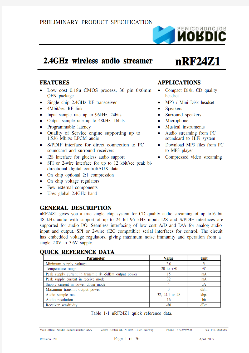
QUICK REFERENCE DATA
Parameter
Value Unit Minimum supply voltage 2.0 V Temperature range
-20 to +80
°C Peak supply current in transmit @ -5dBm output power 15 mA Peak supply current in receive mode 32 mA Supply current in power down mode 4 μA Maximum transmit output power 0
dBm Audio sample rate 32, 44.1 or 48
kbps Audio resolution 16 bit Receiver sensitivity
-80
dBm
Table 1-1 nRF24Z1 quick reference data.
nRF24Z1
ORDERING INFORMATION
Type number Description Version
nRF24Z1 36L QFN 6x6 mm A nRF24Z1-EVKIT Evaluation kit 1.0
Table 1-2 nRF24Z1 ordering information.
TABLE OF CONTENTS FEATURES (1)
APPLICATIONS (1)
GENERAL DESCRIPTION (1)
QUICK REFERENCE DATA (1)
ORDERING INFORMATION (2)
TABLE OF CONTENTS (3)
1 Pin Assignment (6)
2 Pin Function (7)
3 Glossary of terms (8)
4 Architectural Overview (9)
4.1 Audio transmitter (11)
4.1.1 I2S audio input (11)
4.1.2 S/PDIF audio input (12)
4.1.3 Serial control (slave) interfaces (12)
4.1.4 Master interfaces (12)
4.1.5 Direct data input pins (13)
4.1.6 Interrupt output (13)
4.2 Audio Receiver (13)
4.2.1 I2S audio output (14)
4.2.2 S/PDIF audio output (15)
4.2.3 Master interfaces (15)
4.2.4 Serial control (slave) interfaces (15)
4.2.5 Parallel port and PWM (15)
4.3 Blocks common to audio transmitter and receiver (16)
4.3.1 XTAL Oscillator (16)
4.3.2 Radio Transceiver (16)
4.3.3 Quality of Service engine (16)
4.3.4 Audio compression / Decompression (17)
4.3.5 Power (17)
4.3.6 IREF / RESET (17)
5 Operation overview (18)
5.1 Power on / RESET sequence (18)
5.2 RF Link initialization (18)
5.2.1 Idle state (18)
5.2.2 Link-locate state (19)
5.2.3 Synchronization state (19)
5.3 Audio streaming (19)
5.4 Audio receiver clock rate recovery (20)
5.5 Data link (20)
5.6 Power down mode (21)
6 nRF24Z1 register MAP (22)
6.1 Access from audio transmitter side (22)
6.2 Access from audio receiver side (22)
7 Digital I/O (25)
7.1 Digital I/O behaviour during RESET (25)
7.2 Audio interfaces (25)
7.3 I2S Audio Interface (25)
7.4 S/PDIF Audio Interface (26)
7.5 Audio interface functionality (27)
7.5.1 ATX audio interface control (27)
7.5.2 ARX audio interface control (30)
7.5.3 I2S Audio interface timing (32)
7.6 Serial master interfaces (33)
7.6.1 Timing serial master interfaces (36)
7.7 Control and GPIO interfaces (37)
7.7.1 ATX control and GPIO pins (37)
7.7.2 SPI slave interface (38)
7.7.3 2-wire slave interface (38)
7.7.4 General purpose input pins D[2:0] (40)
7.7.5 ATX Control interface timing (41)
7.7.6 ARX control interface options (42)
7.7.7 ARX GPIO pins (43)
7.8 Data Channel Timing (45)
7.8.1 Forward data channel, data transfer from ATX to ARX (45)
7.8.2 Return data channel, data transfer from ARX to ATX (46)
8 Quality of service (Qos) and RF (48)
8.1 Link algorithm (48)
8.2 RF protocol (48)
8.3 Adaptive frequency hopping (48)
8.3.1 Adapting to the RF environment (50)
8.4 Link registers (50)
8.4.1 RF link latency (52)
8.5 RF output power (53)
9 Interrupts (54)
10 RESET outputs (55)
11 Power down control (56)
11.1 Enter power down (56)
11.2 Wake up from power down (56)
11.2.1 External pin change (57)
11.2.2 Timer controlled wake up (57)
11.3 nRF24Z1 power saving example (58)
12 Register update over the data link (60)
13 Eletrical Specification (61)
14 Absolute maximum ratings (63)
15 Package outline (64)
16 Application Information (65)
16.1 Antenna I/O (65)
16.2 Crystal Specification (65)
16.3 Bias reference resistor (65)
16.4 Internal digital supply de-coupling (65)
16.5 PCB layout and de-coupling guidelines (66)
17 Application example (67)
17.1 nRF24Z1 schematics (67)
17.2 nRF24Z1 layout (69)
17.3 nRF24Z1 Bill of Material (71)
18 References (73)
19 Definitions (74)
20 Your notes (75)
1PIN ASSIGNMENT
VDD
VSS
IREF
VSS
VDD
VSS_PA
ANT2
ANT1
XC1
XC2
VSS
DVDD
VSS
WS DATA
CLK
IRQ/
DO[3]/PWM
DD[0]/DI[0]
DD[1]/DI[1]
SMOSI/DD[2]/DI[2]
SCSN/SADR/DI[3]
SSCK/SSCL/DO[0]
SMISO/SSDA/DO[1]
MMOSI MCSN
MMISO
VDD
SSEL/DO[2]
VDD_PA
MSDA
MSCL
SPDIO MCLK
MSCK
REQ
MODE
Figure 1-1: Pin assignment nRF24Z1
2PIN FUNCTION
Name Pin function Description Pin
Slave IF ARX
GPIO Slave IF
ARX
GPIO IF ATX/ARX with slave IF ARX with GPIO IF
1 SSEL DO[2] Dig. In Dig. Out Slave interface select
1: 2-wire, 0: SPI
GPIO out bit #2
2 SMISO
/SSDA DO[1] Digital Output
/ Digital IO
Slave SPI serial out
/ Slave 2-wire data (bidir)
GPIO out bit #1
3 SSCK
/SSCL DO[0] Dig. In Dig. Out Slave SPI clock
/ Slave 2-wire clock
GPIO out bit #0
4 SCSN
/SADR DI3 Digital Input Slave SPI slave select
/ Address select 2-wire slave
GPIO in bit #2
5 VDD Power Power Supply (2.0-3.
6 V DC)
6 SMOSI
/DD[2] DI2 Digital Input Slave SPI serial in
/ Direct data in bit #2
GPIO in bit #3
7 DD[1] DI1 Digital Input Direct data in bit #1 GPIO in bit #1
8 DD[0] DI0 Digital Input Direct data in bit #0 GPIO in bit #0
9 REQ Dig. Out Dig. In I2S data request (programmable polarity)
10 CLK Dig. In Dig. Out I2S bit clock
11 WS Dig. In Dig. Out I2S word clock
12 DATA Dig. In Dig. Out I2S data signal
13 SPDIO Dig. In Dig. Out S/PDIF interface
14 MCLK Dig. Out 256X sample rate clock to ADC or DAC
15 DVDD Regulator output Digital voltage regulator output for decoupling
16 VSS Power Ground (0V)
17 XC2 Analog output Crystal Pin 2
18 XC1 Analog input Crystal Pin 1
19 VDD Power Power Supply (2.0-3.6 V DC)
20 VDD_PA Regulator output DC output (+1.8V) for RF interface (ANT1, ANT2)
21 ANT1 RF Antenna interface 1
22 ANT2 RF Antenna interface 2
23 VSS_PA Power Ground (0V)
24 IREF Analog input Connection to external Bias reference resistor, or RESET
if pulled to VDD
25 VSS Power Ground (0V)
26 MODE Digital Input nRF24Z1 function
1 : audio transmitter, 0: audio receiver
27 MSDA Digital IO Master 2-wire bi-directional data
28 MSCL Digital IO Master 2-wire bi-directional clock
29 MCSN Digital Output Master SPI primary slave select (active low)
30 MMISO Digital Input Master SPI serial input
31 MMOSI Digital Output Master SPI serial output
32 VSS Power Ground (0V)
33 VDD Power Power Supply (2.0-3.6 V DC)
34 VSS Power Ground (0V)
35 MSCK Digital Output Master SPI clock
36 IRQ DO[3]
/ PWM Digital Output Interrupt request GPIO out bit #3
/ PWM output Table 2-1 nRF24Z1 pin function
3GLOSSARY OF TERMS
Term Description
ADC Analog to Digital Converter
ARX audio receiver
ATX audio transmitter
CD Carrier Detect
CHPA SPI clock phase
CLK Clock
CPOL SPI clock polarity
CRC Cyclic Redundancy Check
DAC Digital to Analog Converter
DSP Digital Signal Processor
EEPROM electrical erasable programmable read only
memory
Flash Flash memory
GFSK Gaussian Frequency Shift Keying
GPIO General Purpose In Out
I2S 3 wire audio serial interface
ISM Industrial-Scientific-Medical
LPCM linear PCM (pulse code modulation)
MBZ Must Be Zero (reserved for future extensions)
MCU Micro Controller Unit
MP3 a popular compressed audio format
PWM Pulse Width Modulation
QOS Quality Of Service
RX Receive
S/PDIF one wire serial digital audio format
SPI Serial Peripheral Interface
TX Transmit
2-wire 2-wire serial interface compatible with I2C
Table 3-1 Glossary of terms nRF24Z1.
4ARCHITECTURAL OVERVIEW
nRF24Z1 is a 4 MBit/s single chip RF transceiver that operates in the world wide 2.4 GHz licencee free ISM band. The nR24Z1 is based on the proven nRF24xx radio and ShockBurst? platforms from Nordic Semiconductor.
The device offers a wireless channel for seamless streaming of LPCM or compressed audio in parallel with a low data rate control channel. To enable this, the device offers the following features in addition to the nRF24xx RF platform:
?Standard digital audio interfaces (I2S, S/PDIF)
?Fully embedded Quality of Service engine that handles all RF protocol and RF link tasks.
?SPI and 2-wire master and slave control interfaces
?GPIO pins
As all processing related to audio I/O, RF protocol and RF link management is embedded, the device offers the end application an up to 1.54 MBit/s transparent audio channel without any true time processing needed. nRF24Z1 can be utilized in systems without external microcontroller or by a simple microcontroller that only need to handle low speed tasks over the serial or parallel ports (ex: volume up/down).
A typical system using nRF24Z1 can be seen in Figure 4-1
Audio Source
Audio
transmitter
Figure 4-1 Typical audio application using nRF24Z1
In this system a DSP or micro controller feeds data from storage to nRF24Z1 using standard audio format (I2S). A nRF24Z1 pair transfers the audio data and presents it to a stereo DAC on the other side. For other parts of the application, the nRF24Z1 link will in other words look like an open channel (like a cable).
Initial configuration of nRF24Z1 is done by the micro controller through a SPI or 2-wire control interface. On the destination side, peripherals like a DAC can be controlled from the audio source side through the control channel offered by nRF24Z1. In designs without an external micro controller, configuration data can be loaded by nRF24Z1 from an optional EEPROM/FLASH memory, enabling it to operate stand alone with limited feature set.
A wireless system that is streaming audio will have a very asymmetrical load on the RF link since audio data is fed from an audio source (CD player) to a destination (loud speakers). From the destination back to the audio source only service and control communication is needed.
nRF24Z1 are used both on the audio source side (ex. in a CD player) transmitting audio data, and in the 'destination' (loud speaker) side receiving audio data. Due to the asymmetry, nRF24Z1 has two main modes set by external pin MODE, depending on which side of the link it is put. The two modes have significant differences both in internal and I/O functionality.
To ease understanding of nRF24Z1 operation, the following notation is introduced:
? Audio transmitter (ATX) – nRF24Z1 on the audio source side, transmitting audio data ? Audio receiver (ARX ) – nRF24Z1 on the destination side, receiving audio data
Transmitter and receiver are here referring to the flow of the audio; the nRF24Z1 RF front end always runs a full two way link.
The nRF24Z1 control and data channel is a two way low data rate channel superimposed on the audio and service communication. The audio transmitter is designated master meaning that when a RF link is present 2-wire, SPI, GPIO and internal registers in the audio receiver can be seen and controlled as a virtual extension of the audio transmitters own I/O and registers. The implications of this is that external devices like audio DAC or volume control components connected to the audio receiver effectively can be controlled by input to the audio transmitter. User actions (ex: push of a button) on the audio receiver side are similarly fed back to and can be processed on the audio transmitter side.
The following sections will give an overview of the I/O, main modules and functionality of nRF24Z1. Due to the differences in ATX and ARX, the overview will present the modes separately.
4.1 Audio transmitter
When nRF24Z1 is put at the audio source side of the RF link, MODE must be high and nRF24Z1 becomes an audio transmitter (ATX). The block schematic of nRF24Z1 in ATX mode can be seen in Figure 4-2.
ANT1ANT2VDD_PA
SSDA/SSCL/SMISO SSCK SMOSI/SCSN SPDIO CLK DATA WS MSDA MSCL MMISO MSCK MMOSI MCSN
MCLK XC2XC1
IREF
REQ
VSS_PA VSS VDD DVDD SADR/IRQ SSEL DD[1:0]
DD[2]
Figure 4-2 nRF24Z1 ATX mode block diagram
The I2S or S/PDIF interfaces can be used for audio data input or alternatively the device may stream other real-time data from a DSP over the I2S interface.
4.1.1 I2S audio input
For seamless input from audio sources physically close to nRF24Z1, I2S is the preferred interface. The I2S interface consists of pins CLK, DATA and WS. The interface supports
sample rates of 32, 44.1, 48 and 96 kHz. Data may be in 16, 20 or 24 bit format.1 The data rate is autom atically detected.
I2S may also be used with an external stereo ADC for analog audio sources. The nRF24Z1 offers a 256 times audio sampling rate clock (f S) on the MCLK pin to be used as system clock for the ADC.
A REQ output is available for pacing the data-flow when streaming MP3 and other “data” streams over the I2S interface.
4.1.2S/PDIF audio input
For audio sources physically more remote, the ATX offers a (CMOS level) S/PDIF input on pin SPDIO. This interface supports 32, 44.1 or 48 kHz sampling rates with resolution of 16, 20 or 24 bit. It supports both linear and nonlinear audio according to IEC standards, see ch. 7.4 for details.
4.1.3Serial control (slave) interfaces
When ATX is controlled by an external MCU, configuration and control data both for the audio transmitter itself and a linked audio receiver may be entered via a 2-wire or SPI slave serial interface. The same interface is used for reading back status information. The register map is identical for both interfaces, but only one of the interfaces, selected by SSEL pin, may be used in a given application.
The two interfaces are :
SSEL = 0; SPI (pins SCSN, SSCK, SMISO, SMOSI).
SSEL = 1; 2-wire (pins SADR, SSCL and SSDA)
Pin SADR is not part of a standard 2-wire interface but selects one of two possible bus addresses for the nRF24Z1.
4.1.4Master interfaces
For standalone operation of nRF24Z1, a serial EEPROM or FLASH memory may be connected to a SPI or 2-wire master interface. If a memory is present at any of these interfaces during power up or reset, the device will read default configuration data from the memory.
The SPI master is found on pins MCSN, MMISO, MMOSI and MSCK and 2-wire master on pins MSDA and MSCL.
1 This specification item is for the I2S input interface. Not all of these formats can be transferred within the available 1.54 Mbit/s data rate.
4.1.5Direct data input pins
The ATX has 2 general purpose input pins, DD[1:0], that may be transmitted directly to and hence mirrored on the audio receiver. When SSEL is set high (2-wire interface selected), one additional direct data pin (DD[2]) is available. If the logic level on pins DD[2:0] are mirrored (copied) over the control link, pins DO[2:0] on the a udio receiver will carry the mirrored signal.
These pins may hence be used to switch on/off audio receiver peripherals without microprocessor activity.
4.1.6Interrupt output
The nRF24Z1 can interrupt the external application through pin IRQ based on a number of sources such as no audio input detected, loss of RF communication etc.
Once IRQ has triggered external MCU, interrupt status can be read, through the serial control interface.
4.2 Audio Receiver
When nRF24Z1 is put at the destination side of the RF link, MODE must be low and nRF24Z1 becomes the audio receiver (ARX). The block schematic of nRF24Z1 in ARX mode can be seen in Figure 4-3. I2S or S/PDIF are now used for audio or other real time data output.
MSDA MSCL MMISO MSCK MMOSI MCSN
ANT1ANT2VDD_PA
SPDIO CLK DATA WS MCLK
XC2XC1
IREF
DI[3:0]
DO[3:0]
REQ
VSS_PA VSS
VDD DVDD
Figure 4-3 nRF24Z1 ARX mode block diagram
After a link is established the user can control the SPI and 2 wire master from the audio transmitter. In this way the audio transmitter is able to control audio receiver serial peripherals like audio DACs and amplifiers.
4.2.1 I2S audio output
Audio output to devices physically close to nRF24Z1 (typically a stereo DAC) are normally driven by the I2S output (pins CLK, DATA and WS). The interface supports sample rates of 32, 44.1 and 48 kHz. Data are in 16 bit format.
In audio receiver mode the MCLK pin provides 256 times f S clock for an external DAC.
A REQ input is available for pacing the data-flow when streaming MP3 or other “data” streams over the I2S.
4.2.2S/PDIF audio output
For physically more remote audio devices, the audio receiver provides an S/PDIF (full swing CMOS) output on pin SPDIO. This interface supports 32, 44.1 and 48 kHz, 16 or 24 bit data. It supports both linear and nonlinear audio according to IEC standards, see ch. 7.4 for details.
4.2.3Master interfaces
A serial EEPROM or FLASH memory ma y be connected to a SPI or 2-wire master interface. If a memory is present at any of these interfaces during power up or reset, the device will read default configuration data from that memory; otherwise hard coded default values will be used.
During audio receiver configuration, the SPI master (pins MMSCK, MMISO, MMOSI, MCSN) is operated at 1MHz or 0.5MHz with the SPI format set to CPOL=0,CHPA=0 for EEPROM/FLASH compatibility. After a link is established, the user may control the SPI master from the audio transmitter. The available clock speed is up to 8 MHz over the full operation range of the device.
During start-up, the audio receiver operates the 2-wire master (MSDA, MSCL) interface at 100 kHz. After a link is established, the user may control the 2-wire master from the audio transmitter to 100kHz, 400kHz or 1MHz.
4.2.4Serial control (slave) interfaces
When ARX is controlled by an external MCU, configuration and control data for the audio receiver may be entered via a2-wire or SPI slave serial interface. The same interface is used for reading back status information. The register map is identical for both interfaces, but only one of the interfaces, selected by SSEL pin, may be used in a given application. The two interfaces are :
SSEL = 0; SPI (pins SCSN, SSCK, SMISO, SMOSI).
SSEL = 1; 2-wire (pins SADR, SSCL and SSDA)
Pin SADR is not part of a standard 2-wire interface but selects one of two possible bus addresses for the nRF24Z1.
4.2.5Parallel port and PWM
Alternatively to the serial slave interfaces, ARX can be configured with an 8 bit parallel port, which can be controlled and read from the audio transmitter. There are 4 input pins DI[3:0] that are continuously monitored when a link is up. Changes on any of these inputs will be sent back to the audio transmitter where it can be accessed in a register (via the serial control interface). The audio receiver can also be programmed to wake up from power down mode on a change on one of these pins.
There are 4 outputs DO[3:0] that are controlled from the audio transmitter. Any of these may be programmed for high current in order to drive LEDs or for standard CMOS to control of other devices on the audio receiver board.
DO3 may be programmed to output a PWM signal, where the output duty cycle is programmable with 8-bit resolution from the audio transmitter. Note that this PWM cannot be used as audio DAC
The output pins DO[3:0] may also function as slave select signals if multiple slaves are present on the ARX SPI master bus.
4.3 Blocks common to audio transmitter and receiver
4.3.1XTAL Oscillator
The crystal oscillator will provide a stable reference frequency with low phase noise for the radio and audio functions. See section 16.2 for full Crystal Specification.
4.3.2Radio Transceiver
The RF transceiver part of the circuit is a member of nRF24xx family of low power highly integrated 2.4GHz ShockBurst? transceivers. The transceiver interface is optimized for high speed streaming of up to 4 Mbps. Output power and some protocol parameters can be controlled by the user via the QoS module.
4.3.3Quality of Service engine
The primary function of the quality of service engine is to deliver a robust communication channel between the audio transmitter and audio receiver in an audio streaming application.
Several data streams with different properties are handled. The available bandwidth is shared between audio data, service data and remote data.
Data integrity is ensured through a number of RF protocol features:
1.Packets of data are sent in frames and integrity of each packet is ensured as every
packet has a complete build of RF address, payload and CRC.
2.Packets that are lost or received with errors are handled by the error correction level
of the quality of service engine; a two way, acknowledge protocol:
When a packet is received by ARX, it’s r egistered and CRC is checked.
After ARX has received a frame it sends a packet back to ATX
acknowledging the packets that where successfully transferred. Packets lost
or received with errors will be re-sent from ATX in the next frame.
3.Finally the information (audio data) is spread over the 2.4 GHz band by use of an
adaptive frequency hopping algorithm. Through this a nRF24Z1 link can handle RF propagation challenges like reflections and multi-path fading and not least avoid
heavily trafficked areas of the 2.4 GHz band. The 2.4 GHz band is a world wide open RF band and co-existence with RF systems such as Bluetooth, ZigBee, WLAN/WiFi as well as other nRF applications, is increasingly important.
nRF24Z1 constantly monitors the quality of the RF link and numbers indicating total link quality are available for external control devices in registers. nRF24Z1 can also be set to interrupt external controller devices upon poor link quality before RF link is lost. An external controller device can hence take further actions to improve link quality or warn end user if RF link margins are poor.
The secondary function of the QoS module is to run a link initialization algorithm which manages initial connect and re-connect if link is lost (ex: out of range) between paired nRF24Z1’s. Several schemes are available to enable nRF24Z1 connection without end user involvement.
4.3.4Audio compression / Decompression
Default operation for nRF24Z1 is streaming of uncompressed audio, however there is some optional low delay audio compression options available. This function can be enabled by the user to conserve power or to increase the dynamic range with a constant signal to noise ratio for 24-bit input signals.
4.3.5Power
The power section of nRF24Z1 offers linear regulated supply to all internal parts of the device. This makes the device very robust towards external voltage supply noise and isolates (audio) devices in an application from noise generated the nRF24Z1.
4.3.6IREF / RESET
The IREF pin sets up the bias reference for the nRF24Z1 by use of an external resistor. Pulling IREF to VDD will reset the device. When IREF pin is released, nRF24Z1 runs a full configuration procedure.
5OPERATION OVERVIEW
5.1 Power on / RESET sequence
When supply is applied, nRF24Z1 goes into power on reset. The reset is held until supply voltage is kept above minimum supply voltage for a few milliseconds. Pulling IREF to VDD will also put the device into reset.
When reset (power on or IREF high) is released the device needs to be configured. There are 2 ways nRF24Z1 can be configured:
1.After reset nRF24Z1 will look for an external EEPROM/FLASH memory on the SPI
master interface. If such a memory is present, configuration data is loaded, which means that all registers values are read from the external memory. If no memory is present on the SPI master interface, the procedure is repeated on the 2-wire master interface. These data will override any initial content of nRF24Z1 registers.
2.If no external memory is present:
For both ATX and ARX an external micro processor must configure the nRF24Z1 through the slave SPI or 2-wire serial interface, otherwise hard coded initial register content is used.
NOTE:
A combination of the two power-up sequences may well be used. One likely
scenario is that ATX is configured by external MCU and ARX is configured from an external EEPROM/FLASH memory.
nRF24Z1 will now start a link initialization procedure based on the link configuration data. The value of the MODE pin determines whether it will be in ATX or ARX mode.
5.2 RF Link initialization
Figure 5-1 : link initialisation algorithm
5.2.1Idle state
The nRF24Z1 link initialsation algorithm will be in its idle state when a link is established, and the channel hopping engine is initiated and synchronized.
5.2.2Link-locate state
When the link between ATX and ARX is broken, a special link-locate routine is initiated on both sides to establish a new link, see Figure 5-1. During initialization nRF24Z1 derives a set of channels from register CHP1, CHP2 and CHP3, which will be used during channel hopping in idle state. These channels are also utilized by the link-locate routine when acquiring a feasible startup channel for the new link.
- Link-locate on ATX
ATX tries to establish a link with ARX by iteratively sending short search packages on all available channels until acknowledge is received from ARX. ATX will send one package on each channel and wait for acknowledge for a specific time which i s long enough to secure that ARX has time to respond. The accumulated time used by ATX while looping through all available channels is here defined as the ATX-loop-time. After receiving an acknowledge package from ARX, ATX will enter the synchronization state as described in Figure 5-1.
- Link-locate on ARX
ARX tries to establish a link with ATX by listening for incoming search packages on all available channels until such is received. When a search package is received, ARX will proceed by sending one acknowledge package to confirm a feasible link. ARX will listen for incoming search packages on each channel for a fixed time which is larger than the ATX-loop-time, which will guarantee at least one search package to get through on each available channel used by ARX, as long as this channel is not being occupied by another radio device. After sending the acknowledge package, ARX will enter the synchronization state.
5.2.3Synchronization state
This state takes care of synchronizing the channel hopping engine on ATX and ARX, to secure that both parts follows the same hopping sequence. ATX takes initiative for starting the channel hopping engine, by sending a start condition to ARX about when to start hopping. Which channel to start from is implicitly found during the link-locate state.
5.3 Audio streaming
The audio data fed to the audio interfaces on a nRF24Z1 in ATX mode can be of a number of common digital audio stream formats :
I2S (audio serial) interface:
?left justified, I2S and right justified
S/PDIF interface:
?Consumer Linear PCM Audio described in IEC 60958-3. nRF24Z1 has a single ended CMOS interface, so to fulfil the electrical requirements external adaptation circuitry is needed.
?Non-Linear PCM Audio. As described in IEC 61937-1 (General) and IEC 61937-2 (Burst-info). The nRF24Z1 is transparent to the specific audio compression algorithms used, so it covers all the described formats in IEC 61937-3 to 61937-7.
In ATX the audio stream formats are converted to the nRF24Z1 RF protocol and transferred over the air.
In the ARX the data are validated and converted back to audio stream format and fed to the corresponding audio output interface.
5.4 Audio receiver clock rate recovery
In all RF systems streaming ‘true time’ data, maintaining equal datarates on both sides of RF link, is a big challenge. In other words; keeping the master clock (MCLK) for the DAC on the receiving side, equal to the clock used to feed data into the RF device on the transmitter side.
If these two clocks are not equal the receiving end will either run out of samples for the DAC or overflow hence need to skip some.
Usually this problem is solved by use of very thigh tolerance crystals (expensive) or extensive digital filtering (high current consumption) only masking or interpolating the bits missing in the stream.
nRF24Z1 solves this problem without tight tolerance crystal or extensive digital filtering. As long as the nRF24Z1 quality of service engine is able to maintain a RF link, the ARX (audio receiver) locks its master clock output (MCLK) to the speed the audio stream actually is fed into the ATX on. The MCLK signal on the ARX side is hence locked to the reference (crystal) of the device (DSP, MCU, DECODER) feeding the audio data to the ATX and not the crystal of the nRF24Z1 devices (ATX or ARX) themselves.
One exception; if the MCLK output option is used in audio transmitter (clocking an external ADC for instance) the crystal on the nRF24Z1 in ATX mode is the reference for the audio speed on the entire nRF24Z1 link.
This offers the end application a true loss less audio channel.
5.5 Data link
There is a 2-way, low bit rate, robust, control and data link running in parallel with the audio stream. This data link is a part of the quality of service overhead, i.e. difference between on the air data rate (4 MBit/s) and audio data rate 1.5 MBit/s. Data link rate can hence not be traded for higher audio data rate. The functionality of the control and data link is illustrated in Figure 5-2.
CRB600H钢筋等强度替换表
楼板钢筋等强度替换表一 HRB400 CRB600H 替换 板内替换后钢筋板内原设计钢筋钢筋布置钢筋面积替换钢筋布置钢筋面积 RH6@130 210 替换 8@200 251 RH6@125 222 替换 8@190 265 RH6@120 234 替换 8@180 279 RH8@200 248 替换 8@170 296 RH8@190 263 替换 8@160 314 RH8@170 280 替换 8@150 335 RH8@160 301 替换 8@140 359 RH8@150 324 替换 8@130 387 RH8@140 351 替换 8@120 419 RH8@130 383 替换 8@110 457 RH8@110 421 替换 8@100 503 RH8@100 468 替换 8@90 559 RH8@90 526 替换 8@80 628 RH8@80 601 替换 8@70 718 注: RH表示CRB600H级钢筋,fy=430N/mm2
楼板钢筋等强度替换表二 HRB400 CRB600H 替换 板内替换后钢筋板内原设计钢筋钢筋布置钢筋面积替换钢筋布置钢筋面积 RH8@150 329 替换 10@200 393 RH8@140 346 替换 10@190 413 RH8@130 365 替换 10@180 436 RH10@200 387 替换 10@170 462 RH10@190 411 替换 10@160 491 RH10@170 439 替换 10@150 524 RH10@160 470 替换 10@140 561 RH10@150 506 替换 10@130 604 RH10@140 548 替换 10@120 654 RH10@130 598 替换 10@110 714 RH10@110 657 替换 10@100 785 RH10@100 731 替换 10@90 873 RH10@90 822 替换 10@80 982 RH10@80 939 替换 10@70 1122 注: RH表示CRB600H级钢筋,fy=430N/mm2
浅析替代词
浅析替代词 新建一中秦平 高考中替代词是常考的语法项目,因此,我们对它应有个全面的了解。替代词包括it, one, ones, the one, the ones, that, those 等,其作用就是替代前面某一名词,以避免重复。做关于替代词题的关键所在是弄清楚替代词替代的是哪种名词,可数名词还是不可数名词?单数名词还是复数名词?表特指的名词还是表泛指的名词?下面就上述替代词结合例题来逐一分析。 一. It ①用来替代上文中的同一个物体,请看下面例题: I bought a camera yesterday, and I like it very much. 这里的it 替代的是昨天买的camera,是同一个物体。 ②it作为替代词用在……like /love/hate it when……句型中,用来替代when ……例如: He loves it when she sings. 这个句子中it替代了when she sings, 句意为:他喜欢看她唱歌。[考例]①-----It’s a lovely day, isn’t it? ------Yes. I love ______ when the weather is like this. Why don’t we sit outside and have our lunch? A. this B. that C. it D. one ②I hate when people talk with their mouths full. A. it B. that C. these D. them 简析:这里考查it指代后文中when引导的从句这一功能,因而第①题选C;it 指代when theweather is clear and bright; 第②题选A, it替代when people talk with their mouths full. 二. One /ones (1)替代上文中被不定冠词a/an修饰的单数名词用one 例如:①Do you have a car? Yes, I have one. ②A bridge made of stone is much stronger than one made of wood. 在例一中one替代了a car, 在例二中,one 替代了a bridge. (2)表泛指,指同类事物中的一个(把,件……)用one, 指同类事物中
英语写作中高级同义词替换 2分析
英语写作中高级同义词替换 连词篇:(介词,副词) Firstly: previously, beforehand, foremost, initially, originally, formerly, principally, mainly, essentially, basically, generally, commonly, universally, on the whole, fundamentally, to begin with, to start with Then: subsequently, afterward, thereafter, after that, secondarily, what is more, furthermore (further more)…Lastly:ultimately,eventually, in conclusion, to conclude, as a final point, last of all, last but not least, finally… Too: as well (句末), in addition, besides, moreover, additionally, to boot, excessively, also… And: plus, as well as, along with, in addition, bonus, with… Or: otherwise, if not, before, or else… So(adv): therefore, thus, consequently, accordingly, as a result, for that reason, hence, that’s why Because: as, due to, since, as to, in that, for the reason that, for, now that… But:however, moreover, nevertheless, nonetheless, on the contrary, on the other hand, 让步although, even thought, though, even if, while, as, despite the fact that…
钢筋等截面及等强度代换
钢筋等截面及等强度代换 小 钢筋等截面及等强度代换 钢筋理论重量: 理论重量=0.00617*d^2(kg/m) 强度系数(设计强度): Ⅰ级钢 2.4 Ⅱ级钢 3.4 Ⅲ级钢 3.8 (1)等截面代换:一般指原设计钢筋和代换钢筋的材质(设计强度)相同,但直径不同时的代换,其计算公式为: 代换钢筋间距=(代换钢筋理论重量/原设计钢筋理论重量)*原设计间距 [例]某设计采用了圆10钢筋,间距180mm配筋,因圆10钢筋无货,拟用圆8代换,代换钢筋的间距应是多少? 代换钢筋间距=0.395/0.617*180=115(mm)......... 当施工中遇有钢筋的品种或规格与设计要求不符是,可按钢筋等强度代换、等面积代换原则代换: 1、等强度代换:当构件受强度控制时,钢筋可按强度相等原则进行代换;即不同钢号的钢筋按强度相等的原则代换。即代换后的钢筋强度应大于或等于代换前的钢筋强度; 2、等面积代换:当构件按最小配筋率配筋时,钢筋可按面积相等的原则进行代换。即同钢号的钢筋按钢筋面积相等的原则代换; 3、当构件受裂缝宽度或挠度控制时,代换后进行雷锋宽度或挠度验算; 4、代换后的钢筋应满足构造要求和设计中提出的特殊要求; 钢筋代换时,必须要充分了解设计意图和代换材料性能,并严格遵守现行混凝土结构设计规范的各项规定;凡重要结构中的钢筋代换,要征得设计单位同意。 (1)、对某些重要的构件,如吊车梁、薄腹梁、桁架弦等,不宜用一级光圆钢筋代替二级带肋钢筋; (2)、钢筋替换后,应满足配筋构造规定,如钢筋的最小直径、间距、根数、锚固长度等; (3)、同一截面内,可同时配有不同种类和直径的代换钢筋,但每根钢筋的拉力不应过大,以免构件受力不匀; (4)、梁的纵向受力钢筋与弯起钢筋应分别代换,以保证正截面与斜截面的强度; (5)、偏心受压构件分别代换; (6)、当构件受裂缝宽度控制时,如以小直径钢筋代换大直径钢筋,强度等级低的钢筋代换强度等级高的钢筋,则可不作裂缝宽度验算; 【质量验收要求】 5.1.1 当钢筋的品种、级别或规格需作变更时,应办理设计变更文件。 【相关规范要求】 ①《混凝土结构设计规范》GB 50010—2002 11.2.2 结构构件中的普通纵向受力钢筋宜选用HRB400、HRB335级钢筋;箍筋宜选用HRB335、HRB400、HPB235级钢筋。在施工中,当需要以强度等级较高的钢筋代替
CRB600H钢筋等强度替换表
楼板钢筋等强度替换表一 CRB600H 替换 HRB400 板内替换后钢筋 板内原设计钢筋 钢筋布置 钢筋面积 替换 钢筋布置 钢筋面积 RH 6@130 210 替换 8@200 251 RH 6@125 222 替换 8@190 265 RH 6@120 234 替换 8@180 279 RH 8@200 248 替换 8@170 296 RH 8@190 263 替换 8@160 314 RH 8@170 280 替换 8@150 335 RH 8@160 301 替换 8@140 359 RH 8@150 324 替换 8@130 387 RH 8@140 351 替换 8@120 419 RH 8@130 383 替换 8@110 457 RH 8@110 421 替换 8@100 503 RH 8@100 468 替换 8@90 559 RH 8@90 526 替换 8@80 628 RH 8@80 601 替换 8@70 718 RH 表示CRB600H 级钢筋,fy=430N/mm2 楼板钢筋等强度替换表二 CRB600H 替换 HRB400 板内替换后钢筋 板内原设计钢筋 钢筋布置 钢筋面积 替换 钢筋布置 钢筋面积 RH 8@150 329 替换 10@200 393
RH8@140 346 替换10@190 413 RH8@130 365 替换10@180 436 RH10@200 387 替换10@170 462 RH10@190 411 替换10@160 491 RH10@170 439 替换10@150 524 RH10@160 470 替换10@140 561 RH10@150 506 替换10@130 604 RH10@140 548 替换10@120 654 RH10@130 598 替换10@110 714 RH10@110 657 替换10@100 785 RH10@100 731 替换10@90 873 RH10@90 822 替换10@80 982 RH10@80 939 替换10@70 1122 RH表示CRB600H级钢筋,fy=430N/mm2 楼板钢筋等强度替换表三 CRB600H HRB400 替代 板内替换后钢筋板内原设计钢筋 钢筋布置钢筋面积替代钢筋布置钢筋面积RH10@160 473 替代12@200 565 RH10@150 498 替代12@190 595 RH10@140 526 替代12@180 628 RH12@200 557 替代12@170 665 RH12@190 592 替代12@160 707 RH12@170 631 替代12@150 754 RH12@160 676 替代12@140 808 RH12@150 728 替代12@130 870
连环替代法分析运用
连环替代法的分析运用 某企业2010年3月生产产品所耗某种材料费的实际数就是6720元,而其计划数就是5400元。实际比计划增加1320元。由于材料费用就是由产品产量、单位产品材料耗用量与材料单价三个因素的乘积构成的。因此,可以把材料费用这一总指标分解为三个因素,现假设这三个因素的数值如下表所示。 一、连环替代法之不拿出式 (一)替换顺序:产品产量单位产品材料消耗量材料单价 计划指标:130×10×4=5200(元) ① 第一次替代:140×10×4=5600(元)② 第二次替代:140×9×4=5040(元) ③ 第三次替代得到:140×9×5=6300(元) ④ ②-①=5600-5200=400(元) 产量增加的影响
③-②=5040—5600=-560(元)材料节约的影响 ④-③=6300-5040=1260(元) 价格提高的影响 400-560+1260=1100(元) 全部因素的影响 (二)替换顺序:产品产量材料单价单位产品材料消耗量 计划指标:130×10×4=5200(元) ① 第一次替代:140×10×4=5600(元)② 第二次替代:140×10×5=7000(元) ③ 第三次替代得到:140×9×5=6300(元) ④ ②-①=5600-5200=400(元) 产量增加的影响 ③-②=7000—5600=1400(元)价格提高的影响 ④-③=6300-7000=-700(元)材料节约的影响 400+1400-700=1100(元) 全部因素的影响(三)替换顺序:单位产品材料消耗量产品产量材料单价 计划指标:130×10×4=5200(元) ① 第一次替代:130×9×4=4680(元)② 第二次替代:140×9×4=5040(元) ③ 第三次替代得到:140×9×5=6300(元) ④
因素分析法(连环替代法和差额计算法)
案例分析一一因素分析法(抚钢) 抚顺特殊钢(集团)有限责任公司(下称抚钢)财务分析中常采用因素分析法,即把 某一综合指标分解成若干个相互联系的因素,并分别计算、分析各个因素影响程度的方法。 例如,企业利用 连环替代法 对构成某种钢锭的原材料费用(金属料费用)进行分析, 成本资料列于表1: 由表1可以看出,构成该种钢锭的原材料成本比目标超支了 50 400元,影响这一指 标变动的因素有产量、材料单耗、材料单价三个因素。在这三个因素中,应先替代起决定作 用的产量因素,其次替代派生的单耗因素,最后代替单价因素。分析过程如下: 钢锭中材料费目标总成本 =目标产量X 目标单耗X 材料目标单价 X 1.2 X 870 =2 088 000 (元) (1)替代产量因素=实际产量X 目标单耗X 材料目标单价 =2 296 800 则产量变动对材料成本的影响数值 =2 296 800-2 088 000=208 800( 元) (2) 替代单耗因素=实际产量X 实际单耗X 材料目标单价 =2 200 X 1.08 X 870 =2 067 120 (元) 则单耗变动对材料成本的影响数 =2 067 120-2 296 800=-229 680 (元) (3) 替代单价因素=实际产量X 实际单耗X 材料实际单价 =2 200 X 1.08 X 900 =2 138 400 (元) 则单价变动对材料成本的影响数值 =2 138 400-2 067 120=71 280 (元) 将这三个因素的综合影响数值相加: 208 800+ (-229 680 ) +71 280=50 400 (元) =2 000 =2 200 X 1.2 X 870 (元)
CRBH钢筋等强度替换表
C R B H钢筋等强度替换表 Hessen was revised in January 2021
RH6@130 8@200 RH6@125 8@190 RH6@120 8@180 RH8@200 8@170 RH8@190 8@160 RH8@170 8@150 RH8@160 8@140 RH8@150 8@130 RH8@140 8@120 RH8@130 8@110 RH8@110 8@100 RH8@100 8@90 RH8@90 8@80 RH8@80 8@70 注:RH表示CRB600H级钢筋,fy=430N/mm2
RH8@150 10@200 RH8@140 10@190 RH8@130 10@180 RH10@200 10@170 RH10@190 10@160 RH10@170 10@150 RH10@160 10@140 RH10@150 10@130 RH10@140 10@120 RH10@130 10@110 RH10@110 10@100 RH10@100 10@90 RH10@90 10@80 RH10@80 10@70 注:RH表示CRB600H级钢筋,fy=430N/mm2
RH10@160 12@200 RH10@150 12@190 RH10@140 12@180 RH12@200 12@170 RH12@190 12@160 RH12@170 12@150 RH12@160 12@140 RH12@150 12@130 RH12@140 12@120 RH12@130 12@110 RH12@110 12@100 RH12@100 12@90 RH12@90 12@80 RH12@80 12@70 注:RH表示CRB600H级钢筋,fy=430N/mm2
《学习策略与思维方法》讲座 第七讲 向你推荐替换分析法
《学习策略与思维方法》讲座第七讲向你 推荐替换分析法 第七讲 向你推荐替换分析法 替换分析法是笔者在40余年的数学、物理教学中,运用数学思维处理物理问题的一种解题分析方法。运用这一方法,方便于我们从纷繁复杂的物理情境中,正确地建立物理模型,迅速地确立解题的基本公式,并快捷寻得解题的具体途径和求解的结果。而且,替换分析法的表述式,能直观而简洁地表现出解题的思路,还能极其方便地换写成解题的一般表述形式。 替换分析法不仅可应用于解答物理问题,而且也可用于其它学科有关问题的解题分析。 一、替换分析法的基本思想。 任何一个问题所涉及的各个量中,总分三类:已知的,未知但为所求的,未知但非所求的。已知的为已知量,未知但为所求的称所求量,未知但非所求的为称不求量。解题就是要依据符合问题规定情境的有关规律,运用已知量,化去不求量,求出所求量。数学方程论告诉我们:一个方程只能求一个未知量,通常n个方程构成的方程组也只能求n个未
知量。其中超量的不求量必须化去,化去的方法总是进行这样的替换,用含已知量、所求量的解析式替换不求量,使原方程得以变形。而这种量的替换通常要进行到所得方程的个数与未知量的个数相等为止,则此方程或方程组可解,即其中所求未知量可以求出。 替换分析法就是通过这种量的替换来寻求解题的具体途径的一种解题分析方法。 二、替换分析法的操作步骤。 利用替换分析法解物理问题,一般可分两步进行: 根据题所提供的物理情境,建立物理模型,恰当地选择物体或物体系,并根据其所处的物理状态或物理过程,优选一个物理公式作为解题的基本公式。 为了解题的简捷,选作解题的基本公式不仅要满足题给的物理情境,还应满足如下条件:①尽可能含所求量;②尽可能多含已知量;③尽可能少含不求量。 如果所选的某个基本公式只含一个所求量,其余均为已知量,不含任何不求量,则此基本公式是关于所求量的一元方程,可直接求出相应所求量,故此公式为解此题的最佳基本公式。若解题的基本公式不是最佳的,则应进行下述有关不求量的替换。 对解题的基本公式中的不求量进行分析替换,使之成为关于所求量的可解方程或可解方程组。分析替换的原则是,
替换电阻的分析方法
1.在图11所示的电路中,电源电压为12伏且不变,电阻R 1的阻值为22欧,滑动变阻器R 2上标有“10 1A ”字样。闭合电键S ,电流 表的示数为0.5安。求: (1)电阻R 1两端的电压。 (2)滑动变阻器R 2接入电路的阻值。 (3)现设想用定值电阻R 0来替换电阻R 1, 要求:在移动滑动变阻器滑片P 的过程中,两 电表的指针分别能达到满刻度处,且电路能正常工作。 ①现有阻值为16欧的定值电阻,若用它替换电阻R 1,请判断:________满足题目要求(选填“能”或“不能”)。若能满足题目要求,通过计算求出替换后滑动变阻器的使用范围;若不能满足题目要求,通过计算说明理由。 ②满足题目要求的定值电阻R 0的可能取值范围为_______________________。 (1)U 1=IR 1 =0.5安×22欧=11伏 (2)R 2=U 2/I 2=(U -U 1)/I =(12伏-11伏)/0.5安=2欧 (3)①能; 电流表量程为0~0.6安: 由I 最大=0.6安, R 最小=12伏/0.6安=20欧, 图11 A R 1 P V R 2 S
R 滑小=20欧-16欧=4欧; 由U 滑大=3伏, U 1 =U -U 滑大=12伏-3伏=9伏, I =U 1/R 0=9伏/16欧≈0.563安, R 滑大=U 滑大/I =3伏/0.563安≈5.33欧, 所以,滑动变阻器使用范围:4~5.33欧。 ②R 0的取值范围为15~20欧。 2.在图11所示的电路中,电源电压保持不变,滑动变阻器R 2上标有 “100Ω 1A ”字样。闭合电键S 后,电流表A 的示数为 0.5安,电压表V l 的示数为10伏,电压表V 2的示数为6伏。求: ①定值电阻R 1的阻值。 ②此时滑动变阻器R 2消耗的电功率P 2。 图11 ③请用定值电阻来替换电阻R 1,并选择合适的电表量程。要求:在不更换电表量程的情况下,移动变阻器的滑片P ,使所有电表的示数都能达到各自的最大值,且电路能正常工作。 第一,符合上述条件的所有可能的定值电阻阻值:__________________。 第二,满足上述要求时,电流表示数的最小值。(写 明必要理由) A V 2 V 1 R 1 R 2 S P
钢筋替换规则
钢筋代换与钢筋代换原则 当施工中遇有钢筋的品种或规格与设计要求不符是,可按钢筋等强度代换、等面积代换原则代换: 1、等强度代换:当构件受强度控制时,钢筋可按强度相等原则进行代换;即不同钢号的钢筋按强度相等的原则代换。即代换后的钢筋强度应大于或等于代换前的钢筋强度; 2、等面积代换:当构件按最小配筋率配筋时,钢筋可按面积相等的原则进行代换。即同钢号的钢筋按钢筋面积相等的原则代换; 3、当构件受裂缝宽度或挠度控制时,代换后进行宽度或挠度验算; 4、代换后的钢筋应满足构造要求和设计中提出的特殊要求; 钢筋代换时,必须要充分了解设计意图和代换材料性能,并严格遵守现行混凝土结构设计规范的各项规定;凡重要结构中的钢筋代换,要征得设计单位同意。 (1)、对某些重要的构件,如吊车梁、薄腹梁、桁架弦等,不宜用一级光圆钢筋代替二级带肋钢筋; (2)、钢筋替换后,应满足配筋构造规定,如钢筋的最小直径、间距、根数、锚固长度等; (3)、同一截面内,可同时配有不同种类和直径的代换钢筋,但每根钢筋的拉力不应过大,以免构件受力不匀; (4)、梁的纵向受力钢筋与弯起钢筋应分别代换,以保证正截面与斜截面的强度; (5)、偏心受压构件分别代换; (6)、当构件受裂缝宽度控制时,如以小直径钢筋代换大直径钢筋,强度等
级低的钢筋代换强度等级高的钢筋,则可不作裂缝宽度验算。 另外代换的时候不能私自代换,因为牵涉到工程量变更和签证的问题,所以在代换前要和监理沟通,不能擅自做主代换!如果不是因为材料短缺的话建议不要代换,这些事很麻烦.上过这类事情的当, 如果是桥面铺装,这一部分桥面铺装参加箱梁或者空心板梁的顶板共同受力,计算中考虑了强度,那么就不能换,另,如果是预应力箱梁或者预应力T 梁腹板处的箍筋,在规范里属于强制性条文,是不许换的。 螺纹钢换成光圆的钢筋,比较重大,必须有设计代表同意。慎重,慎重。
CRBH钢筋等强度替换表
RH 6@130 8@200 RH 6@125 8@190 RH 6@120 8@180 RH 8@200 8@170 RH 8@190 8@160 RH 8@170 8@150 RH 8@160 8@140 RH 8@150 8@130 RH 8@140 8@120 RH 8@130 8@110 RH 8@110 8@100 RH 8@100 8@90 RH 8@90 8@80 RH 8@80 8@70 注: RH 表示CRB600H 级钢筋,fy=430N/mm2 钢筋布置 钢筋布置 RH 8@150 10@200
RH8@140 10@190 RH8@130 10@180 RH10@200 10@170 RH10@190 10@160 RH10@170 10@150 RH10@160 10@140 RH10@150 10@130 RH10@140 10@120 RH10@130 10@110 RH10@110 10@100 RH10@100 10@90 RH10@90 10@80 RH10@80 10@70 注:RH表示CRB600H级钢筋,fy=430N/mm2 RH10@160 12@200 RH10@150 12@190 RH10@140 12@180 RH12@200 12@170 RH12@190 12@160 RH12@170 12@150 RH12@160 12@140 RH12@150 12@130
RH12@140 12@120 RH12@130 12@110 RH12@110 12@100 RH12@100 12@90 RH12@90 12@80 RH12@80 12@70 注:RH表示CRB600H级钢筋,fy=430N/mm2
因素分析法(连环替代法和差额计算法)
案例分析——因素分析法(抚钢) 抚顺特殊钢(集团)有限责任公司(下称抚钢)财务分析中常采用因素分析法,即把某一综合指标分解成若干个相互联系的因素,并分别计算、分析各个因素影响程度的方法。 例如,企业利用连环替代法对构成某种钢锭的原材料费用(金属料费用)进行分析,成本资料列于表1: 由表1可以看出,构成该种钢锭的原材料成本比目标超支了50 400元,影响这一指标变动的因素有产量、材料单耗、材料单价三个因素。在这三个因素中,应先替代起决定作用的产量因素,其次替代派生的单耗因素,最后代替单价因素。分析过程如下:钢锭中材料费目标总成本=目标产量×目标单耗×材料目标单价 =2 000×1.2×870 =2 088 000(元) (1)替代产量因素=实际产量×目标单耗×材料目标单价 =2 200×1.2×870 =2 296 800(元) 则产量变动对材料成本的影响数值=2 296 800-2 088 000=208 800(元) (2)替代单耗因素=实际产量×实际单耗×材料目标单价 =2 200×1.08×870 =2 067 120(元) 则单耗变动对材料成本的影响数=2 067 120-2 296 800=-229 680(元) (3)替代单价因素=实际产量×实际单耗×材料实际单价 =2 200×1.08×900 =2 138 400(元) 则单价变动对材料成本的影响数值=2 138 400-2 067 120=71 280(元) 将这三个因素的综合影响数值相加: 208 800+(-229 680)+71 280=50 400(元) 分析结果表明,该钢锭的实际材料成本比目标成本超支了50 400元。主要原因是:
钢筋等强代换
钢筋理论重量: 强度系数(设计强度); Ⅰ级钢 2.4 Ⅱ级钢 3.4 Ⅲ级钢 3.8 (1)等截面代换:一般指原设计钢筋和代换钢筋的材质(设计强度)相同,但直径不同时的代换,其计算公式为: 代换钢筋间距=(代换钢筋理论重量/原设计钢筋理论重量)*原设计间距 [例] 某设计采用了圆10钢筋,间距180mm配筋,因圆10钢筋无货,拟用圆8代换,代换钢筋间距应是多少? 代换钢筋间距=0.395/0.617*180=115(mm) (2)按理论重量代换钢筋根数:适用于采用跟数配筋时,计算公式为: 代换钢筋根数≧原设计钢筋理论重量/代换钢筋理论重量*原设计根数 [例] 某设计配筋为10根圆10,拟用圆8代换,代换后应是多少根? 代换钢筋根数=0.617/0.395*10=15.62,取定16根。 采用根数代换时,一定要注意构造要求。 (3)等强度带换:一般指原设计钢筋与代换钢筋的规格(直径)相同或者不同,但材质(设计强度)不同时的代换,其计算公式为: 代换钢筋间距=(代换钢筋理论重量*代换钢筋强度系数)/(原设计钢筋理论重量*原设计钢筋强度系数)*原设计间距(mm) [例] 原设计圆10间距180mm(Ⅰ级钢),现采用圆8代换(Ⅱ级钢),代换钢筋的间距应是多少? 代换钢筋间距=(0.395*3.4)/(0.617*2.4)*180=163(mm) (4)按强度代换钢筋根数:适用于设计采用根数配筋时,计算公式如下: 代换钢筋根数≧(原设计钢筋理论重量*原设计钢筋强度系数)/(代换钢筋理论重量/代换钢筋强度系数)*原设计根数 [例] 原设计采用4根圆25(Ⅰ级钢),若用圆22(Ⅱ级钢)代换钢筋,需要几根? 代换钢筋根数=(3.85*2.4)/(2.98*3.4)*4=3.65,取定4根
替换电阻专题(含解析)
替换电阻专题 一、知识结构 串联电路: 各电表都达到了满刻度(定值电阻与滑变器) 每次移动都能使得电表处于某一位置 每次移动都使得电表改变得角度相同 并联电路: 各电表都达到了满刻度(定值电阻与滑变器) 通过电键得断开与闭合使得各电表满刻度 替换后两个电表偏离零刻度线得角度相同两个电流表得比值相同电表得指针始终处于某一个位置 二、题型 类型一:电压表接在滑动变阻器得两端 1、在图所示得电路中,电源电压为12伏且不变,电阻R1得阻值为22欧,滑动变阻器R2上标有“10Ω1A”字样.闭合电键S,电流表得示数为0、5安.求: (1)电阻R1两端得电压. (2)滑动变阻器R2接入电路得阻值. (3)现设想用定值电阻R0来替换电阻R1,要求:在移动滑动变阻器滑片P得过程中,两电表得指针分别能达到满刻度处,且电路能正常工作. ①现有阻值为16欧得定值电阻,若用它替换电阻R1,请判断:能满足题目要求(选填“能”或“不能”).若能满足题目要求,通过计算求出替换后滑动变阻器得使用范围;若不能满足题目要求,通过计算说明理由. ②满足题目要求得定值电阻R0得可能取值范围为15~20Ω. 分析:②当滑动变阻器接入电路得电阻最小时,电路中得电流最大为0、6A,根据欧姆定律求出R0得最大阻值;当滑动变阻器接入电路得电阻最大时,电流表得示数也最大时,电阻R0得阻值最小,利用串联电路得电压特点与欧姆定律求出最小值,从而确定足题目 要求得定值电阻R0得可能取值范围. 解答:解:(3)①能; 电流表量程为0~0、6A,即I最大=0、6A, 此时电路中得总电阻R最小===20Ω, 滑动变阻器接入电路得最小值R滑小=20Ω﹣16Ω=4Ω; 电压表得量程为0~3V,即U滑大=3V, 定值电阻两端得电压U1′=U﹣U滑大=12V﹣3V=9V, 电路中得电流I′===0、5625A, 滑动变阻器接入电路得最大值R滑大==≈5、33Ω, 所以,滑动变阻器使用范围:4Ω~5、33Ω. ②当滑动变阻器接入电路得电阻最小为0,电路中得电流最大I max=0、6A时,R0得阻值最大; R0max===20Ω, 当滑动变阻器接入电路得电阻最大时,电流表得示数也最大时,R0得阻值最小; R0min===15Ω, 所以R0得取值范围为15Ω~20Ω. 答:(1)电阻R1两端得电压为11V; (2)滑动变阻器R2接入电路得阻值为2Ω; (3)①能;替换后滑动变阻器得使用范围为4Ω~5、33Ω; ②满足题目要求得定值电阻R0得可能取值范围为15Ω~20Ω. 点评:本题考查了串联电路得特点与欧姆定律得计算;关键就是规律与公式得灵活运用;难点就是满足题目要求得定值电阻R0得取值范围得确定. 类型2:电压表接在定值电阻两端: 2、在图(a)电路中,电源电压为18伏且不变.电阻R1得阻值30欧,滑动变阻器R2上标有“20Ω2A”字样.闭合电键S,电压表得示数为12伏. (1)求电流表得示数. (2)求电阻R2连入电路得阻值. (3)若移动变阻器滑片P到某位置时,发现两电表中某一个表得指针达到满刻度,如图(b)或(c)所示. ①求出此时两电表得示数. ②现要求在移动变阻器滑片P时两电表得指针均能达到满刻度,如图(b)与(c)所示,小华与小明拟采取如下方法: 小华:用5欧得定值电阻替换电阻R1. 小明:用25欧得定值电阻替换电阻R1. 请判断:小明得方法能满足题目得要求(选填“小华”、“小明”或“小华与小明”).满足题目要求时,滑动变阻器连入电路得阻值R2得值为5欧. ③继续移动变阻器得滑片P,直至电路中电流最小,则两电表指针偏转角度得变化量就是相同得(选填“相同”或“不同”).
CRBH钢筋等强度替换表
C R B H钢筋等强度替换 表 集团标准化办公室:[VV986T-J682P28-JP266L8-68PNN]
RH6@130 8@200 RH6@125 8@190 RH6@120 8@180 RH8@200 8@170 RH8@190 8@160 RH8@170 8@150 RH8@160 8@140 RH8@150 8@130 RH8@140 8@120 RH8@130 8@110 RH8@110 8@100 RH8@100 8@90 RH8@90 8@80 RH8@80 8@70 注:RH表示CRB600H级钢筋,fy=430N/mm2
RH8@150 10@200 RH8@140 10@190 RH8@130 10@180 RH10@200 10@170 RH10@190 10@160 RH10@170 10@150 RH10@160 10@140 RH10@150 10@130 RH10@140 10@120 RH10@130 10@110 RH10@110 10@100 RH10@100 10@90 RH10@90 10@80 RH10@80 10@70 注:RH表示CRB600H级钢筋,fy=430N/mm2
RH10@160 12@200 RH10@150 12@190 RH10@140 12@180 RH12@200 12@170 RH12@190 12@160 RH12@170 12@150 RH12@160 12@140 RH12@150 12@130 RH12@140 12@120 RH12@130 12@110 RH12@110 12@100 RH12@100 12@90 RH12@90 12@80 RH12@80 12@70 注:RH表示CRB600H级钢筋,fy=430N/mm2
CRBH钢筋等强度替换表
RH6@130 8@200 RH6@125 8@190 RH6@120 8@180 RH8@200 8@170 RH8@190 8@160 RH8@170 8@150 RH8@160 8@140 RH8@150 8@130 RH8@140 8@120 RH8@130 8@110 RH8@110 8@100 RH8@100 8@90 RH8@90 8@80 RH8@80 8@70 注:RH表示CRB600H级钢筋,fy=430N/mm2
RH8@150 10@200 RH8@140 10@190 RH8@130 10@180 RH10@200 10@170 RH10@190 10@160 RH10@170 10@150 RH10@160 10@140 RH10@150 10@130 RH10@140 10@120 RH10@130 10@110 RH10@110 10@100 RH10@100 10@90 RH10@90 10@80 RH10@80 10@70 注:RH表示CRB600H级钢筋,fy=430N/mm2
RH10@160 12@200 RH10@150 12@190 RH10@140 12@180 RH12@200 12@170 RH12@190 12@160 RH12@170 12@150 RH12@160 12@140 RH12@150 12@130 RH12@140 12@120 RH12@130 12@110 RH12@110 12@100 RH12@100 12@90 RH12@90 12@80 RH12@80 12@70 注:RH表示CRB600H级钢筋,fy=430N/mm2
钢筋等截面及等强度代换
钢筋等截面及等强度代换中小小 钢筋等截面及等强度代换钢筋理论重量: 理论重量=0.00617*dA2 ( kg/m ) 强度系数(设计强度): 级钢 2.4 级钢 3.4 级钢 3.8 (1 )等截面代换:一般指原设计钢筋和代换钢筋的材质(设计强度)相同,但直径不同时的代换,其计算公式为: 代换钢筋间距=(代换钢筋理论重量/原设计钢筋理论重量)*原设计间距 [例]某设计采用了圆10钢筋,间距180mm配筋,因圆10钢筋无货,拟用圆8代换,代换钢筋的间距应是多少? 代换钢筋间距=0.395/0.617*180=115 (mm ) 当施工中遇有钢筋的品种或规格与设计要求不符是,可按钢筋等强度代换、等面积代换原则代换: 1、等强度代换:当构件受强度控制时,钢筋可按强度相等原则进行代换;即不同钢号的钢筋按强 度相等的原则代换。即代换后的钢筋强度应大于或等于代换前的钢筋强度; 2、等面积代换:当构件按最小配筋率配筋时,钢筋可按面积相等的原则进行代换。即同钢号的 钢筋按钢筋面积相等的原则代换; 3、当构件受裂缝宽度或挠度控制时,代换后进行雷锋宽度或挠度验算; 4、代换后的钢筋应满足构造要求和设计中提出的特殊要求; 钢筋代换时,必须要充分了解设计意图和代换材料性能,并严格遵守现行混凝土结构设计规范的各项规定;凡重要结构中的钢筋代换,要征得设计单位同意。 (1)、对某些重要的构件,如吊车梁、薄腹梁、桁架弦等,不宜用一级光圆钢筋代替二级带肋钢 筋; (2)、钢筋替换后,应满足配筋构造规定,如钢筋的最小直径、间距、根数、锚固长度等; (3)、同一截面内,可同时配有不同种类和直径的代换钢筋,但每根钢筋的拉力不应过大,以免 构件受力不匀; (4)、梁的纵向受力钢筋与弯起钢筋应分别代换,以保证正截面与斜截面的强度; (5)、偏心受压构件分别代换; (6)、当构件受裂缝宽度控制时,如以小直径钢筋代换大直径钢筋,强度等级低的钢筋代换强度 等级高的钢筋,则可不作裂缝宽度验算; 【质量验收要求】 5.1. 1当钢筋的品种、级别或规格需作变更时,应办理设计变更文件。 【相关规范要求】 ①《混凝土结构设计规范》GB 50010 —2002 11 .2.2结构构件中的普通纵向受力钢筋宜选用HRB400、HRB335级钢筋;箍筋宜选用HRB335、 HRB400、HPB235级钢筋。在施工中,当需要以强度等级较高的钢筋代替原设计中的纵向受力钢筋时, 应按钢筋受拉承载力设计值相等的原则进行代换,并应满足正常使用极限状态和抗震构造措施的要求。
英语中“替代”的用法分析总结-精选范文
英语中“替代”的用法分析总结 替代是一种避免重复的连接上下文的手段。在英语中主要有三种替代现象:名词性替代、动词性替代和分句性替代;同理,替代词也分为名词替代词、动词替代词和分句替代词。此外还有状语的替代。以下是小编为大家整理的“替代”的用法分析总结,希望能帮助大家提高英语水平。 一、名词性替代 用名词性替代词one (s), the same, the kind, the sort 等所表示的替代现象叫做名词性替代。 1.名词性替代词 例1:His novel is a bad one for children. (one = novel)
例2:The child doesn’t like this book. Show him a more interesting one. (one = book) 2.某些不定代词 在名词性替代中还可以用一些不定代词来替代。如all, both, some, any, enough, several, none, many, much, more, (the ) most, (a) few, another, the other, others, either等。例如: I don't want any more food. I’ve had enough. 3. one 和 ones是最常见的替代词 one的复数形式是ones.one 和ones作为替代词只能用
以替代可数名词,不可用来替代不可数名词。例如: 1)The grey horse is stronger than the black one. 2)The new design is much better than the old ones. 4.名词性物主代词mine,yours 名词性物主代词mine, yours等可用来代替my +名词,your +名词等,例如: “Whose is that coat?” “It’s mine.” 二、动词性替代
CRB600H钢筋等强度替换表
C R B600H钢筋等强度替换表 (总3页) -CAL-FENGHAI.-(YICAI)-Company One1 -CAL-本页仅作为文档封面,使用请直接删除
RH6@1308@200 RH6@1258@190 RH6@1208@180 RH8@2008@170 RH8@1908@160 RH8@1708@150 RH8@1608@140 RH8@1508@130 RH8@1408@120 RH8@1308@110 RH8@1108@100 RH8@1008@90 RH8@908@80 RH8@808@70注:RH表示CRB600H级钢筋,fy=430N/mm2
RH8@15010@200 RH8@14010@190 RH8@13010@180 RH10@20010@170 RH10@19010@160 RH10@17010@150 RH10@16010@140 RH10@15010@130 RH10@14010@120 RH10@13010@110 RH10@11010@100 RH10@10010@90 RH10@9010@80 RH10@8010@70注:RH表示CRB600H级钢筋,fy=430N/mm2
RH10@16012@200 RH10@15012@190 RH10@14012@180 RH12@20012@170 RH12@19012@160 RH12@17012@150 RH12@16012@140 RH12@15012@130 RH12@14012@120 RH12@13012@110 RH12@11012@100 RH12@10012@90 RH12@9012@80 RH12@8012@70注:RH表示CRB600H级钢筋,fy=430N/mm2