ME9926

GENERAL DESCRIPTION
The ME9926 is the Dual N-Channel logic enhancement mode power field effect transistors are produced using high cell density, DMOS trench technology. This high density process is especially tailored to minimize on-state resistance. These devices are particularly suited for low voltage application such as cellular phone and notebook computer power management and other battery powered circuits where high-side switching and low in-line power loss are needed in a very small outline surface mount package.
FEATURES
● 20V/6.0A,R DS(ON)=29m ?@V GS =4.5V ● 20V/5.2A,R DS(ON)=42m ?@V GS =2.5V
● Super high density cell design for extremely low R DS(ON) ● Exceptional on-resistance and maximum DC current capability
APPLICATIONS
● Power Management in Note book ● Portable Equipment ● Battery Powered System ● DC/DC Converter ● Load Switch ● DSC
● LCD Display inverter
PIN CONFIGURATION
(SOP-8) Top View
Absolute Maximum Ratings (T A =25℃ Unless Otherwise Noted)
Parameter Symbol Steady State Unit
Drain-Source Voltage V DSS 20 V
Gate-Source Voltage V GSS ±12 V
Continuous Drain Current I D 6 A
Pulsed Drain Current I DM 30 A T A =25℃ 2.0 Maximum Power Dissipation T A =70℃
P D 1.3 W Operating Junction Temperature
T J -55 to 150
℃ R θJA
T≦10 sec
55
℃/W Thermal Resistance-Junction to Ambient * Steady State 88
Thermal Resistance-Junction to Case
R θJC 50
℃/W
e * The device mounted on 1in 2 FR4 board with 2 oz copper
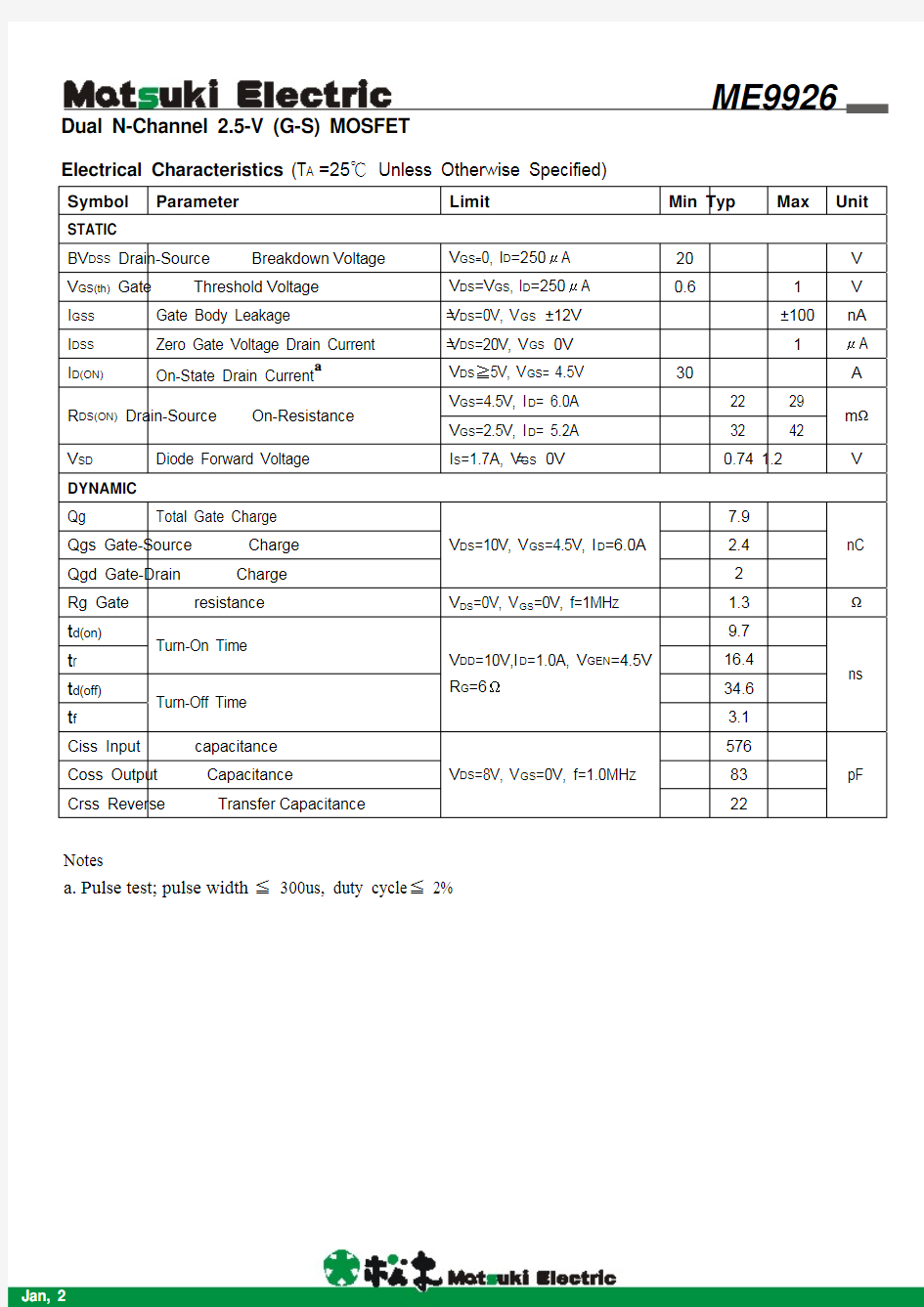
Electrical Characteristics (T A =25℃ Unless Otherwise Specified)
Symbol
Parameter Limit
Min Typ Max Unit
STATIC
BV DSS Drain-Source Breakdown Voltage V GS=0, I D =250μA 20 V V GS(th) Gate Threshold Voltage V DS =V GS , I D =250μA
0.6 1 V
I GSS Gate Body Leakage
V DS =0V, V GS =±12V ±100nA I DSS Zero Gate Voltage Drain Current V DS =20V, V GS =
0V 1 μA I D(ON)
On-State Drain Current
a
V DS ≧5V, V GS = 4.5V 30 A V GS =4.5V, I D = 6.0A 22 29 R DS(ON) Drain-Source On-Resistance V GS =2.5V, I D = 5.2A
32
42
m ?
V SD Diode Forward Voltage
I S =1.7A, V GS =
0V
0.74 1.2 V
DYNAMIC Qg
Total Gate Charge
7.9 Qgs Gate-Source Charge 2.4 Qgd Gate-Drain Charge V DS =10V, V GS =4.5V, I D =6.0A
2 nC Rg Gate resistance
V DS =0V, V GS =0V, f=1MHz 1.3 ? t d(on) 9.7 t r Turn-On Time
16.4 t d(off) 34.6 t f
Turn-Off Time
V DD =10V,I D =1.0A, V GEN =4.5V R G =6Ω
3.1 ns
Ciss Input capacitance
576 Coss Output Capacitance
83 Crss Reverse Transfer Capacitance
V DS =8V, V GS =0V, f=1.0MHz
22
pF
Notes a. Pulse test; pulse width ≦ 300us, duty cycle ≦ 2%
Typical Characteristics (T J =25℃ Noted)
Typical Characteristics (T J =25℃ Noted)
SOP-8 Package Outline
MILLIMETERS
DIM
MIN MAX
A 1.35 1.75
A1 0.10 0.25
B 0.35 0.49
C 0.18 0.25
D 4.80 5.00
E 3.80 4.00
BSC
e 1.27
H 5.80 6.20
h 0.25 0.50
L 0.40 1.25
θ0°7°