AF4407PS中文资料

P-Channel Enhancement Mode Power MOSFET
Features
- Simple Drive Requirement - Low On-resistance
- Fast Switching Characteristic
Product Summary
BV DSS (V)
R DS(ON) (m ?)
I D (A)
-30 9 -14
Pin Assignments
SO-8
D D D D
S S S G
General Description
The advanced power MOSFET provides the designer with the best combination of fast switching, ruggedized device design, low on-resistance and cost-effectiveness.
The SO-8 package is universally preferred for all commercial-industrial surface mount applications and suited for low voltage applications such as DC/DC converters.
Pin Descriptions
Pin Name
Description
S Source
G Gate D Drain
Ordering information
F :MOSFET
S: SO-8
Blank : Normal
L : Lead Free Package
Blank : Tube or Bulk A : Tape & Reel
P-Channel Enhancement Mode Power MOSFET
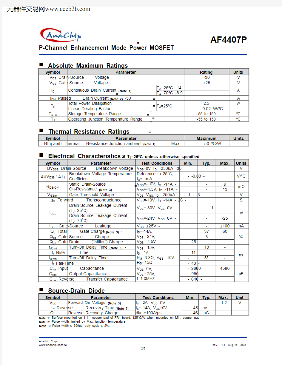
Absolute Maximum Ratings
Symbol Parameter Rating Units
V DS Drain-Source Voltage -30 V V GS Gate-Source Voltage
±25 V
T A =25oC -14
I D Continuous Drain Current (Note 1) T A =70oC -8.9 A
I DM Pulsed Drain Current (Note 2) -50 A Total Power Dissipation 2.5 W
P D Linear Derating Factor T A =25oC 0.02 W/oC
T STG Storage Temperature Range -55 to 150 oC T J Operating Junction Temperature Range -55 to 150 oC
Thermal Resistance Ratings
Symbol Parameter Maximum Units
Rthj-amb Thermal Resistance Junction-ambient (Note 1) Max.
50 oC/W
Electrical Characteristics at T J =25oC unless otherwise specified
Symbol Parameter Test Conditions Min. Typ. Max. Units BV DSS Drain-Source Breakdown Voltage V GS =0V, I D =
-250uA -30 - - V
?BV DSS / ?T J
Breakdown Voltage Temperature Coefficient
Reference to 25o C,
I D =-1mA - -0.03 - V/o C V GS =-10V, I D =
-14A - - 9 R DS(ON)
Static Drain-Source On-Resistance (Note 3) V GS =-4.5V, I D =-11A - - 13
m ?V GS(th) Gate Threshold Voltage V DS =V GS , I D =
-250uA -1 - -3 V g fs Forward Transconductance V DS =-10V, I D =
-14A - 26 - S
Drain-Source Leakage Current
(T J =25o C)
V DS =-30V, V GS =
0V - - -1
I DSS
Drain-Source Leakage Current
(T J =70o C)
V DS =-24V, V GS =
0V - - -25
uA I GSS Gate-Source Leakage V GS =
±25V - - ±100 nA Q g Total Gate Charge (Note 3) - 37 60 Q gs Gate-Source Charge - 3 - Q gd Gate-Drain (“Miller”) Charge I D =-14A,
V DS =-24V, V GS =-4.5V - 25 - nC
t d(on) Turn-On Delay Time (Note 3) - 13 - t r Rise Time - 11 -
t d(off) Turn-Off Delay Time - 58 - t f Fall-Time V DS =-15V,
I D =-1A, R G =3.3?, V GS =-10V R D =15? - 43 -
ns
C iss Input Capacitance - 2860 4580 C oss Output Capacitance - 950 - C rss Reverse Transfer Capacitance
V GS =0V,
V DS =-25V, f=1.0MHz - 640 - pF
Source-Drain Diode
Symbol Parameter Test Conditions Min.Typ. Max. Unit
V SD Forward On Voltage (Note 3) I S =-2A, V GS =
0V - - -1.2 V
t rr Reverse Recovery Time (Note 3) - 48 - ns Q rr Reverse Recovery Charge I S =-14A, V GS =0V, dl/dt=100A/μs - 46 - nC
Note 1: Surface mounted on 1 in 2
copper pad of FR4 board; 125o
C/W when mounted on Min. copper pad.
Note 2: Pulse width limited by Max. junction temperature. Note 3: Pulse width ≤ 300us, duty cycle ≤ 2%.
P-Channel Enhancement Mode Power MOSFET Typical Performance Characteristics
P-Channel Enhancement Mode Power MOSFET
Typical Performance Characteristics (Continued)
P-Channel Enhancement Mode Power MOSFET
Marking Information
SO-8
( Top View )
4 4 0 7 P
"A~Z": 27~52
AA Y W
"A~Z": 27~52
~
Package Information
Package Type: SO-8
1. All Dimensions Are in Millimeters.
2. Dimension Does Not Include Mold Protrusions.
Dimensions In Millimeters
Symbol
Min. Nom. Max.
A 1.35 1.55 1.75
A1 0.10 0.18 0.25
B 0.33 0.41 0.51
C 0.19 0.22 0.25
D 4.80 4.90 5.00
E 5.80 6.15 6.50
E1 3.80 3.90 4.00
L 0.38 0.71 1.27
θ0o4o8o
TYP.
e 1.27