PHP78NQ03LT中文资料

1.Product pro?le
1.1General description
Logic level N-channel enhancement mode Field-Effect Transistor (FET) in a plastic package using T renchMOS technology.
1.2Features
1.3Applications
1.4Quick reference data
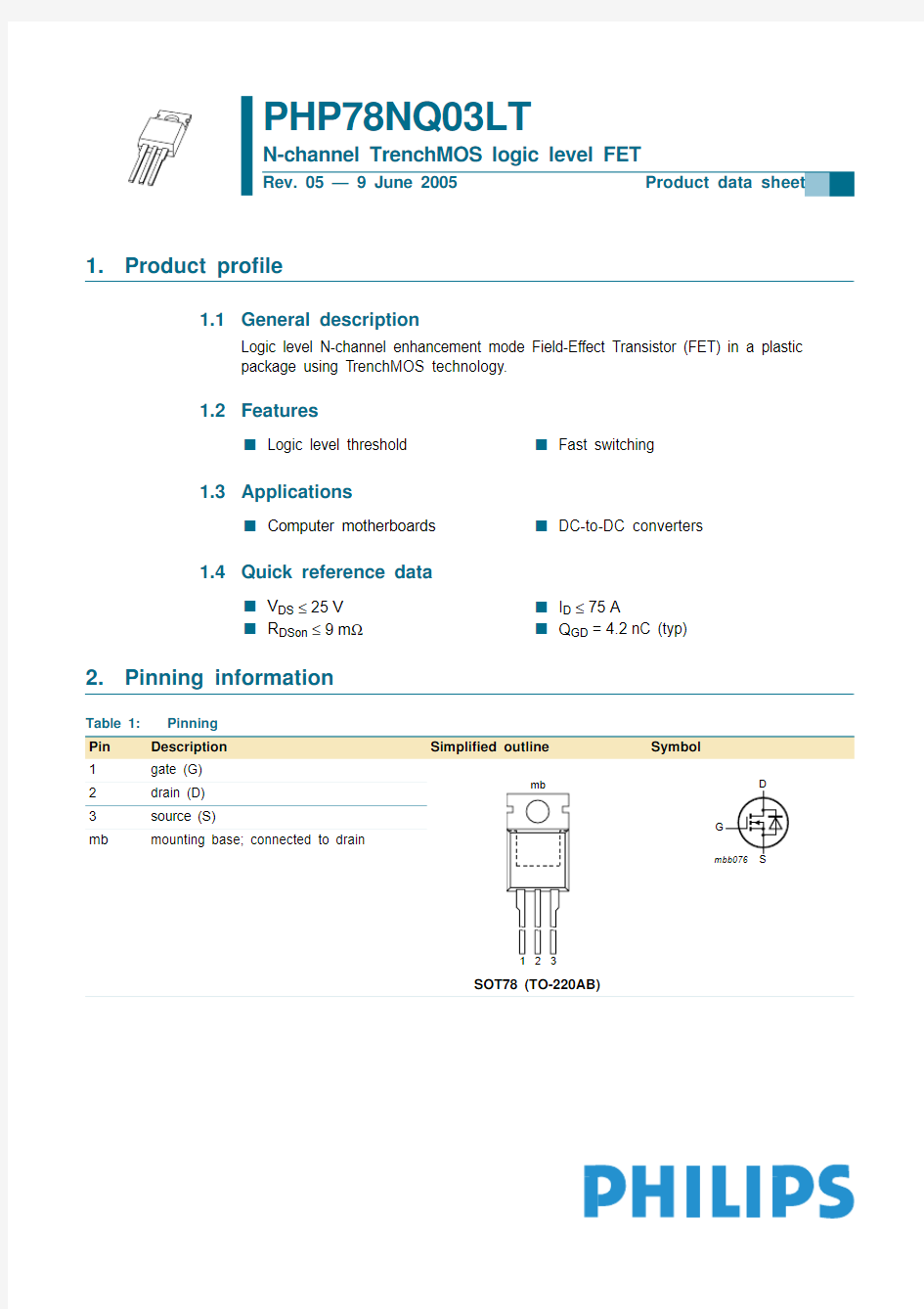
2.Pinning information
PHP78NQ03LT
N-channel TrenchMOS logic level FET
Rev. 05 — 9 June 2005
Product data sheet
s Logic level threshold
s Fast switching
s Computer motherboards
s DC-to-DC converters
s V DS ≤25V s I D ≤75A
s R DSon ≤9m ?
s Q GD =4.2nC (typ)
Table 1: Pinning Pin Description Simpli?ed outline Symbol
1gate (G)SOT78 (TO-220AB)
2drain (D)3source (S)
mb
mounting base; connected to drain
12mb
3
S
D
G
mbb076
3.Ordering information
4.Limiting values
Table 2:
Ordering information
Type number
Package Name
Description
Version PHP78NQ03LT
SC-46
plastic single-ended package; heatsink mounted; 1 mounting hole; 3-lead TO-220AB
SOT78
Table 3:Limiting values
In accordance with the Absolute Maximum Rating System (IEC 60134).Symbol Parameter Conditions Min Max Unit V DS drain-source voltage 25°C ≤T j ≤175°C
-25V V DGR drain-gate voltage 25°C ≤T j ≤175°C; R GS =20k ?
-25V V GS gate-source voltage -±20V I D
drain current
T mb =25°C; V GS =5V;Figure 2 and 3-61A T mb =100°C; V GS =5V;Figure 2-43A T mb =25°C; V GS =10V -75A T mb =100°C; V GS =10V
-53A I DM peak drain current T mb =25°C; pulsed; t p ≤10μs;Figure 3-228A P tot total power dissipation T mb =25°C;Figure 1-93W T stg storage temperature ?55+175°C T j junction temperature
?55+175°C Source-drain diode
I S source (diode forward) current
T mb =25°C
-75A I SM
peak source (diode forward) current T mb =25°C; pulsed; t p ≤10μs
-228A Avalanche ruggedness
E DS(AL)S non-repetitive drain-source
avalanche energy
unclamped inductive load; I D =43A;t p =0.25ms; V DD ≤25V; R GS =50?;V GS =10V; starting at T j =25°C
-185
mJ
Fig 1.Normalized total power dissipation as a
function of mounting base temperature
Fig 2.Normalized continuous drain current as a
function of mounting base temperature
T mb =25°C; I DM is single pulse; V GS =5V
Fig 3.Safe operating area; continuous and peak drain currents as a function of drain-source voltage
03aa16
04080
120050100150
200
T mb (°C)
P der (%)03aa24
40
80
120050100150
200
T mb (°C)
I der (%)P der P tot
P tot 25C °
()
-----------------------100%
×=I der I D
I D 25C °
()
-------------------100%
×=003aaa175
1
10
102
103 1
10
102
V DS (V)
I D (A)t p = 10 μs
DC 100 ms
10 ms Limit R DSon = V DS / I D
1 ms 100 μs
5.Thermal characteristics
Table 4:Thermal characteristics
Symbol Parameter
Conditions Min Typ Max Unit R th(j-mb)thermal resistance from junction to mounting base Figure 4-- 1.6K/W R th(j-a)
thermal resistance from junction to ambient
vertical in still air
-60
-K/W
Fig 4.Transient thermal impedance from junction to mounting base as a function of pulse duration
003aaa233
10-2
10-1 1
1010-5
10-410-310-210-1
1
10
t p (s)
Z th(j-mb)(K/W)single pulse
δ = 0.50.20.1
0.050.02
t p
T
P
t
t p T
δ =
6.Characteristics
Table 5:Characteristics
T j=25°C unless otherwise speci?ed.
Symbol Parameter Conditions Min Typ Max Unit Static characteristics
V(BR)DSS drain-source breakdown voltage I D=250μA; V GS=0V
T j=25°C25--V
T j=?55°C22--V
V GS(th)gate-source threshold voltage I D=1mA; V DS=V GS;Figure9 and10
T j=25°C1 1.52V
T j=175°C0.5--V
T j=?55°C-- 2.2V
I DSS drain-source leakage current V DS=25V; V GS=0V
T j=25°C--10μA
T j=150°C--500μA I GSS gate-source leakage current V GS=±15V; V DS=0V-10100nA R DSon drain-source on-state resistance V GS=5V; I D=25A;Figure6 and8
T j=25°C-11.513.5m?
T j=175°C-20.724.3m?
V GS=10V; I D=25A;Figure6 and8-7.659m?Dynamic characteristics
Q G(tot)total gate charge I D=50A; V DS=15V; V GS=5V;
Figure11-13-nC
Q GS gate-source charge- 4.8-nC Q GD gate-drain (Miller) charge- 4.2 5.6nC
C iss input capacitance V GS=0V; V DS=25V; f=1MHz;
Figure13-1074-pF
C oss output capacitance-389-pF C rss reverse transfer capacitance-156-pF
t d(on)turn-on delay time V DS=15V; R L=0.6?; V GS=10V;
R G=5.6?-2033ns
t r rise time-92130ns t d(off)turn-off delay time-3048ns t f fall time-4060ns Source-drain diode
V SD source-drain(diode forward)voltage I S=25A; V GS=0V;Figure12-0.95 1.2V
t rr reverse recovery time I S=20A; dI S/dt=?100A/μs; V GS=0V;
V R=25V -40-ns
Q r recovered charge-32-nC
T j =25°C T j =25°C
Fig 5.Output characteristics: drain current as a
function of drain-source voltage; typical values
Fig 6.Drain-source on-state resistance as a function
of drain current; typical values
T j =25°C and 175°C; V DS >I D ×R DSon
Fig 7.Transfer characteristics: drain current as a
function of gate-source voltage; typical values
Fig 8.Normalized drain-source on-state resistance factor as a function of junction temperature
003aaa169
020
40
600
0.5
1
1.5
2
V DS (V)
I D (A)V GS = 3 V
3.5 V
4 V
6 V 4.5 V 5 V
10 V 003aaa171
00.02
0.04
0.060
20
40
60
I D (A)
R DSon (?) 4 V
6 V
V GS = 3 V 10 V
5 V 3.5 V
003aaa170
10
2030
40123
4
V GS (V)
I D (A)V DS > I D x R DSon
T j = 25 °C
175 °C 03af18
00.5
1
1.5
2-60
060120
180
T j (°C)
a a R
DSon R DSon 25C °()
----------------------------=
I D =1mA; V DS =V GS T j =25°C; V DS =5V
Fig 9.Gate-source threshold voltage as a function of
junction temperature
Fig 10.Sub-threshold drain current as a function of
gate-source voltage
I D =50A; V DS =15V
Fig 11.Gate-source voltage as a function of gate charge; typical values
03aa33
00.5
11.5
2
2.5-60
060120
180
T j (°C)
V GS(th)(V)
max
typ
min 03aa36
10-6
10-5
10-4
10-3
10-2
10-1012
3
V GS (V)
I D (A)max
typ
min
003aaa174
2
4
6
8
100102030
40
Q G (nC)
V GS (V)
T j =25°C and 175°C; V GS =0V V GS =0V; f =1MHz
Fig 12.Source (diode forward) current as a function of
source-drain (diode forward) voltage; typical values Fig 13.Input,output and reverse transfer capacitances
as a function of drain-source voltage; typical values
003aaa173
10
20
30
4000.40.8 1.2
1.6
V SD (V)
I S (A)T j = 25 °C
175 °C
003aaa172
102
103
104
10-1
1 10
102
V DS (V)
C (pF)
C iss
C oss C rss
7.Package outline
Fig 14. Package outline SOT78 (TO-220AB)
REFERENCES
OUTLINE VERSION EUROPEAN PROJECTION
ISSUE DATE IEC
JEDEC JEITA SOT78
SC-46
3-lead TO-220AB
D
D 1
q
p
L
123
L 1(1)
b 1
e e
b
0510 mm
scale
Plastic single-ended package; heatsink mounted; 1 mounting hole; 3-lead TO-220AB
SOT78
DIMENSIONS (mm are the original dimensions)A E A 1
c
Q
L 2
UNIT A 1b 1D 1e p mm
2.54
q Q A b D c L 2max.3.0
3.83.5
15.012.8
3.302.79
3.02.7
2.62.2
0.70.4
16.015.2
0.90.6
1.451.00
4.74.1
1.401.25
6.65.9
10.39.7
L 1E L 05-01-3105-03-22
mounting base
8.Revision history Table 6:Revision history
Document ID Release
date Data sheet
status
Change
notice
Document
number
Supersedes
PHP78NQ03LT_520050609Product
data sheet
-9397 750 15086PHP_PHU78NQ03LT_4
Modi?cations:?The format of this data sheet has been redesigned to comply with the new
presentation and information standard of Philips Semiconductors.
?Removal of PHU78NQ03LT (now in separate data sheet).
PHP_PHU78NQ03LT_420040726Product
data sheet
-9397 750 13431PHP_PHB_PHD78NQ03LT_3
PHP_PHB_PHD78NQ03LT_320020626Product
data sheet
-9397 750 09667PHP_PHB_PHD78NQ03LT_2
PHP_PHB_PHD78NQ03LT_220020322Product
data sheet
-9397 750 09418PHP_PHB_PHD78NQ03LT_1
PHP_PHB_PHD78NQ03LT_120011114Product
data sheet
-9397 750 08916-
9.Data sheet status
[1]Please consult the most recently issued data sheet before initiating or completing a design.
[2]The product status of the device(s) described in this data sheet may have changed since this data sheet was published. The latest information is available on the Internet at URL https://www.wendangku.net/doc/8913964004.html,.
[3]
For data sheets describing multiple type numbers, the highest-level product status determines the data sheet status.
10.De?nitions
Short-form speci?cation —The data in a short-form speci?cation is extracted from a full data sheet with the same type number and title. For detailed information see the relevant data sheet or data handbook.
Limiting values de?nition — Limiting values given are in accordance with the Absolute Maximum Rating System (IEC 60134). Stress above one or more of the limiting values may cause permanent damage to the device.These are stress ratings only and operation of the device at these or at any other conditions above those given in the Characteristics sections of the speci?cation is not implied. Exposure to limiting values for extended periods may affect device reliability.
Application information — Applications that are described herein for any of these products are for illustrative purposes only. Philips Semiconductors make no representation or warranty that such applications will be suitable for the speci?ed use without further testing or modi?cation.
11.Disclaimers
Life support —These products are not designed for use in life support appliances, devices, or systems where malfunction of these products can reasonably be expected to result in personal injury. Philips Semiconductors
customers using or selling these products for use in such applications do so at their own risk and agree to fully indemnify Philips Semiconductors for any damages resulting from such application.
Right to make changes —Philips Semiconductors reserves the right to make changes in the products - including circuits, standard cells, and/or software - described or contained herein in order to improve design and/or performance. When the product is in full production (status ‘Production’),relevant changes will be communicated via a Customer Product/Process Change Noti?cation (CPCN). Philips Semiconductors assumes no
responsibility or liability for the use of any of these products, conveys no license or title under any patent, copyright, or mask work right to these
products,and makes no representations or warranties that these products are free from patent,copyright,or mask work right infringement,unless otherwise speci?ed.
12.Trademarks
Notice —All referenced brands, product names, service names and trademarks are the property of their respective owners.
TrenchMOS —is a trademark of Koninklijke Philips Electronics N.V .
13.Contact information
For additional information, please visit: https://www.wendangku.net/doc/8913964004.html,
For sales of?ce addresses, send an email to: sales.addresses@https://www.wendangku.net/doc/8913964004.html,
Level Data sheet status [1]Product status [2][3]De?nition
I Objective data Development This data sheet contains data from the objective speci?cation for product development. Philips Semiconductors reserves the right to change the speci?cation in any manner without notice.
II
Preliminary data
Quali?cation
This data sheet contains data from the preliminary speci?cation.Supplementary data will be published at a later date.Philips Semiconductors reserves the right to change the speci?cation without notice,in order to improve the design and supply the best possible product.
III Product data Production
This data sheet contains data from the product speci?cation. Philips Semiconductors reserves the right to make changes at any time in order to improve the design,manufacturing and supply.Relevant changes will be communicated via a Customer Product/Process Change Noti?cation (CPCN).
14.Contents
1Product pro?le. . . . . . . . . . . . . . . . . . . . . . . . . . 1
1.1General description. . . . . . . . . . . . . . . . . . . . . . 1
1.2Features . . . . . . . . . . . . . . . . . . . . . . . . . . . . . . 1
1.3Applications . . . . . . . . . . . . . . . . . . . . . . . . . . . 1
1.4Quick reference data. . . . . . . . . . . . . . . . . . . . . 1
2Pinning information. . . . . . . . . . . . . . . . . . . . . . 1
3Ordering information. . . . . . . . . . . . . . . . . . . . . 2
4Limiting values. . . . . . . . . . . . . . . . . . . . . . . . . . 2
5Thermal characteristics. . . . . . . . . . . . . . . . . . . 4
6Characteristics. . . . . . . . . . . . . . . . . . . . . . . . . . 5
7Package outline . . . . . . . . . . . . . . . . . . . . . . . . . 9
8Revision history. . . . . . . . . . . . . . . . . . . . . . . . 10
9Data sheet status. . . . . . . . . . . . . . . . . . . . . . . 11
10De?nitions . . . . . . . . . . . . . . . . . . . . . . . . . . . . 11
11Disclaimers. . . . . . . . . . . . . . . . . . . . . . . . . . . . 11
12Trademarks. . . . . . . . . . . . . . . . . . . . . . . . . . . . 11
13Contact information . . . . . . . . . . . . . . . . . . . . 11
? Koninklijke Philips Electronics N.V.2005
All rights are reserved.Reproduction in whole or in part is prohibited without the prior
written consent of the copyright owner.The information presented in this document does
not form part of any quotation or contract,is believed to be accurate and reliable and may
be changed without notice.No liability will be accepted by the publisher for any
consequence of its use.Publication thereof does not convey nor imply any license under
patent- or other industrial or intellectual property rights.
Date of release: 9 June 2005
Document number: 9397 750 15086