AMMP-6420中文资料

This preliminary data is provided to assist you in the evaluation of product(s) currently under development. Until Agilent Technologies
releases this product for general sales, Agilent Technologies reserves the right to alter prices, specifications, features, capabilities, functions, release dates, and remove availability of the product(s) at anytime.
Revision Date: 4/28/04 Preliminary Information
AMMP-6420
6-18 GHz 1W Power Amplifier
Data Sheet
Features
? 5x5mm Surface Mount Package ? Wide Frequency Range 6-18 GHz ? One Watt Output Power ? High Gain ? Partially Matched
? DC Supply Bias at 5V, -1V, 700 mA ? Integrated Output Power Detector
Applications
? Microwave Radio systems
? Satellite VSAT and DBS systems ? Commercial grade military
? 802.16 & 802.20 WiMax BWA systems ? WLL and MMDS loops
AMMP-6420: DC & RF Specifications
Sym Parameters/Conditions Typ.
Min/
Max V d Drain Supply Voltage V 5 V g Gate Voltage V -0.8 I D
Drain Supply Current
mA
750
800
Gain Small-signal Gain dB 19 15 RL in Input Return Loss dB -5 RL out Output Return Loss dB
-5
P-1dB
Comp
dBm 29 27 Isol Reverse Isolation dB -30 -25 OIP3 Output 3rd Order Int Point dBm +39
Vdet
Power Detector Voltage
V/W
0.2
Description Agilent’s AMMP-6420 is a high gain amplifier in a surface mount package that operates from 6 to 18 GHz. It is a cost-effective alternative in commercial communications systems to discrete FET hybrid or MIC amplifiers. The MMIC has a partial input and output match to 50? (-5dB typical return loss) but can be easily externally matched by single element lossy or reactive means (inductor or capacitor) for 20%frequency coverage (or 100% coverage if used in a balance configuration with Lange coupler) The MMIC is unconditionally stable over all frequencies and bias conditions. Bias can be applied from either side. Gate voltage is set using the Vg pin to optimize for linear or saturated power amplification. A reference and output detector allows differential output power detection over 15 dB of range. It is fabricated in a PHEMT process to provide exceptional power
and gain performance. GND
BASE Pin
Function
1 V g
2 V d
3 DET o
4 RF Out
5 DET R
6 V d
7 V g
8 RF In
This preliminary data is provided to assist you in the evaluation of product(s) currently under development. Until Agilent Technologies releases this product for general sales, Agilent Technologies reserves the right to alter prices, specifications, features, capabilities, functions, release dates, and remove availability of the product(s) at anytime.
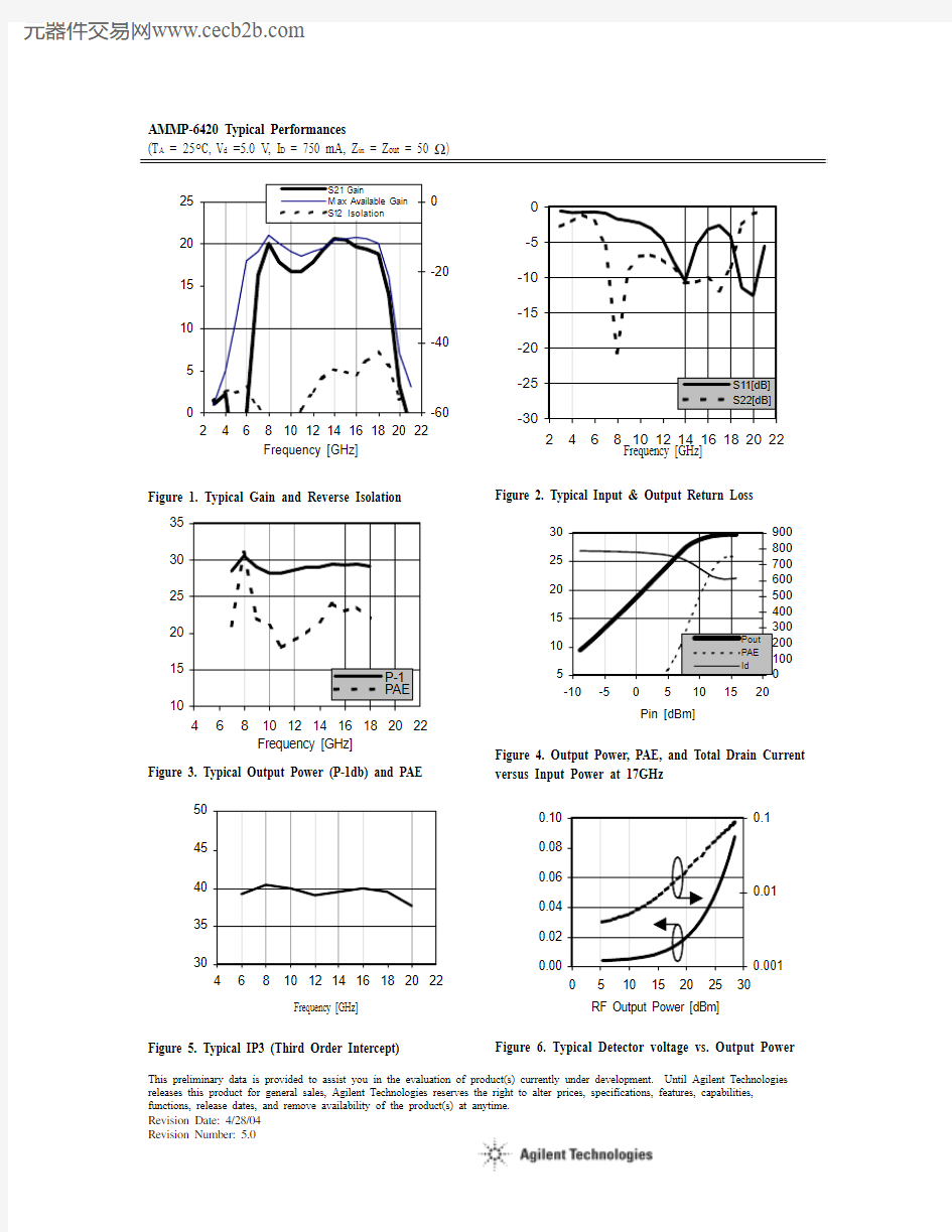
Revision Date: 4/28/04 AMMP-6420 Typical Performances
(T A = 25°C, V d =5.0 V, I D = 750 mA, Z in = Z out = 50 ?)
0510
1520
25G a i n [d B ]
-60
-40
-20
I s o l a t i o n [d B ]
Figure 1. Typical Gain and Reverse Isolation
10
152********
6
810121416182022Frequency [GHz]
P -1 [d B m ], P A E [%]
Figure 3. Typical Output Power (P-1db) and PAE
30
35404550
4
6
8
10121416182022Frequency [GHz]
I P 3 [d B m ]
Figure 5. Typical IP3 (Third Order Intercept)
-30
-25
-20-15-10-502
4
6
810121416182022Frequency [GHz]
R e t u r n L o s s [d B ]
Figure 2. Typical Input & Output Return Loss
51015202530-10
-5
5
10
15
20
Pin [dBm]
P o u t [d B m ], P A E [%]
I d [m A ]
Figure 4. Output Power, PAE, and Total Drain Current versus Input Power at 17GHz
0.00
0.020.040.06
0.080.100
5
10
15
20
25
30
RF Output Power [dBm]
(D E T _R )-(D E T _O ) [V ]
0.001
0.01
0.1
(D E T _R )-(D E T _O ) [V ]]
Figure 6. Typical Detector voltage vs. Output Power
This preliminary data is provided to assist you in the evaluation of product(s) currently under development. Until Agilent Technologies releases this product for general sales, Agilent Technologies reserves the right to alter prices, specifications, features, capabilities, functions, release dates, and remove availability of the product(s) at anytime.
Revision Date: 4/28/04 Typical Scattering Parameters [1], (T A = 25°C, V d =5.0 V, I D = 750 mA, Z in = Z out = 50 ?) Freq S11 S21 S12 S22
[GHz] dB Mag Phase dB Mag Phase dB Mag Phase dB Mag Phase
1 -0.87 0.91 -54.11 -22.86 0.07-38.55-85.330.0001169.56-0.50 0.94 -57.011.5 -1.45 0.85 -77.5
2 -29.09 0.04-78.78-80.940.0001-175.18-0.48 0.95 -83.042 -2.05 0.79 -98.38 -38.89 0.01-86.10-800.000.00000.00-0.48 0.95 -107.242.5 -2.60 0.74 -117.02 -52.07 0.00-13.41-74.510.000282.70-0.5
3 0.9
4 -129.933 -3.13 0.70 -133.84 -40.04 0.01132.81-95.110.0000-5.03-0.59 0.93 -151.463.
5 -3.63 0.6
6 -149.08 -25.5
7 0.05137.83-95.240.0000-70.69-0.79 0.91 -172.694 -4.16 0.62 -162.85 -14.7
8 0.18122.75-79.980.0001160.38-1.18 0.87 165.394.5 -4.71 0.58 -174.8
9 -5.24 0.5596.22-80.180.0001-76.68-1.99 0.80 141.755 -5.29 0.54 175.16 3.44 1.4956.13-74.190.0002-71.45-3.83 0.64 114.075.5 -5.73 0.52 167.60 10.58 3.380.78-68.600.0004-155.78-8.60 0.37 77.296 -5.85 0.51 161.58 14.63 5.39-64.52-63.480.0007161.36-24.98 0.06 -87.526.5 -5.65 0.52 155.54 15.64 6.05-123.83-62.900.0007110.41-8.61 0.37 -165.367 -5.19 0.55 148.54 15.42 5.90-171.25-62.760.000764.88-5.31 0.54 165.397.5 -4.68 0.58 139.87 15.06 5.66149.79-61.900.000821.69-4.11 0.62 143.618 -4.25 0.61 130.07 14.92 5.57115.92-61.140.0009-15.34-3.72 0.65 125.208.5 -3.96 0.63 119.80 15.07 5.6784.71-61.190.0009-53.65-3.80 0.65 108.209 -3.79 0.65 109.47 15.48 5.9454.35-59.700.0010-84.79-4.23 0.61 92.399.5 -3.70 0.65 99.32 16.07 6.3623.93-57.700.0013-118.53-5.08 0.56 77.7610 -3.65 0.66 89.33 16.76 6.88-7.01-55.710.0016-148.81-6.27 0.49 64.4610.5 -3.61 0.66 79.50 17.47 7.47-38.42-54.000.0020179.69-7.79 0.41 52.9411 -3.55 0.66 69.50 18.24 8.16-70.18-51.890.0025150.91-9.71 0.33 43.0411.5 -3.44 0.67 58.76 19.13 9.05-102.74-50.210.0031120.36-12.29 0.24 32.5212 -3.37 0.68 46.60 20.22 10.26-137.44-48.360.003889.71-17.94 0.13 20.3512.5 -3.45 0.67 32.92 21.28 11.59-176.87-47.000.004557.43-23.00 0.07 162.5713 -3.85 0.64 13.79 21.40 11.75142.33-44.150.006230.43-9.62 0.33 135.1413.5 -5.88 0.51 0.42 21.48 11.8699.76-43.540.0067-17.97-5.26 0.55 106.8814 -7.35 0.43 -5.47 20.42 10.5057.22-44.620.0059-59.39-3.42 0.67 80.1914.5 -8.02 0.40 -11.98 19.04 8.9520.45-45.600.0052-92.99-2.93 0.71 56.9115 -8.42 0.38 -22.81 17.91 7.86-12.89-46.420.0048-124.14-3.03 0.71 36.8215.5 -9.02 0.35 -38.63 17.16 7.21-45.24-46.760.0046-155.91-3.50 0.67 18.4416 -9.99 0.32 -59.66 16.76 6.89-78.40-46.650.0047172.05-4.24 0.61 0.8416.5 -11.32 0.27 -88.81 16.62 6.78-113.79-46.210.0049135.75-5.30 0.54 -16.8017 -12.58 0.23 -129.48 16.57 6.74-152.21-45.930.005197.60-6.89 0.45 -35.3617.5 -12.37 0.24 -178.96 16.45 6.64165.77-45.340.005454.57-9.41 0.34 -55.0718 -10.42 0.30 135.67 16.04 6.34119.59-45.720.00529.79-14.81 0.18 -71.0218.5 -8.13 0.39 98.32 15.07 5.6769.37-46.750.0046-42.66-21.32 0.09 -2.6719 -6.44 0.48 64.76 13.21 4.5816.14-49.850.0032-99.91-10.63 0.29 -0.1419.5 -5.54 0.53 32.49 10.33 3.29-37.14-54.540.0019-174.42-6.40 0.48 -35.3620 -5.33 0.54 -0.33 6.65 2.15-88.56-54.970.0018100.12-4.59 0.59 -73.8220.5 -5.63 0.52 -37.08 2.37 1.31-138.35-52.190.002536.40-3.75 0.65 -110.9121 -6.21 0.49 -81.51 -2.59 0.74172.10-51.290.0027-8.72-3.30 0.68 -145.0621.5 -6.54 0.47 -133.73 -8.62 0.37123.31-51.190.0028-48.36-2.95 0.71 -175.6722 -6.04 0.50 176.00 -16.11 0.1677.94-52.060.0025-86.25-2.57 0.74 158.1922.5 -5.17 0.55 136.35 -25.54 0.0538.87-55.520.0017-123.07-2.27 0.77 135.9223 -4.42 0.60 107.30 -38.98 0.0125.37-59.020.0011-141.45-1.99 0.80 116.6723.5 -3.84 0.64 85.86 -42.63 0.0195.60-64.940.0006-153.62-1.77 0.82 100.5024 -3.39 0.68 68.76 -40.35 0.0172.97-76.410.0002-154.09-1.57 0.83 86.1024.5 -3.03 0.71 54.55 -42.31 0.0137.28-72.380.0002-115.43-1.39 0.85 73.3425 -2.78 0.73 42.25 -45.89 0.01 6.70-77.300.0001-145.84-1.25 0.87 62.1625.5 -2.61 0.74 31.43 -49.21 0.00
-19.68
-69.79
0.0003
-11.93
-1.16 0.88 51.84
This preliminary data is provided to assist you in the evaluation of product(s) currently under development. Until Agilent Technologies releases this product for general sales, Agilent Technologies reserves the right to alter prices, specifications, features, capabilities, functions, release dates, and remove availability of the product(s) at anytime.
Revision Date: 4/28/04
Outline Drawing
Suggested PCB Material and Land Pattern
Evaluation Test Circuit (Demo Board)
(Available to customer on qualified request)
Recommended SMT Attachment
The AMMP Packaged Devices are compatible with high volume surface mount PCB assembly processes.
The PCB material and mounting pattern, as defined in the data sheet, optimizes RF performance and is
strongly recommended. An electronic drawing of the land pattern is available from https://www.wendangku.net/doc/8514200214.html,/view/rf or upon request from Agilent Application Engineering.
Manual Assembly for Prototypes
1. Follow ESD precautions while handling packages.
2. Handling should be along the edges with tweezers
or from topside if using a vacuum collet.
3. Recommended attachment is solder paste. Please
see recommended solder reflow profile.
Conductive epoxy is not recommended. Hand soldering is not recommended.
4. Apply solder paste using either a stencil printer or
dot placement. The volume of solder paste will be dependent on PCB and component layout and should be controlled to ensure consistent mechanical and electrical performance.
Excessive solder will degrade RF performance. 5. Follow solder paste and vendor’s
recommendations when developing a solder reflow profile. A standard profile will have a steady ramp up from room temperature to the pre-heat temperature to avoid damage due to thermal shock.
6. Packages have been qualified to withstand a peak
temperature of 235°C for 15 seconds. Verify that the profile will not expose device beyond these limits.
7. Clean off flux per vendor’s recommendations. 8. Clean the module with Acetone. Rinse with
alcohol. Allow the module to fully dry before
testing.
For product information and a complete list of Agilent contacts and distributors, please go to our website: https://www.wendangku.net/doc/8514200214.html,/semiconductors
E-mail: SemiconductorSupport@https://www.wendangku.net/doc/8514200214.html, Data subject to change.
Copyright ? 2004 Agilent Technologies, Inc.
NOTES:
1. ? INIDICATES PIN 1
2.
DIMENSIONS ARE IN INCHES [MILIMETERS]3.
ALL GROUNDS MUST BE SOLDERED TO PCB RF GROUND