CY7C4291-10JI中文资料

64K/128K x 9 Deep Sync FIFOs
CY7C4281CY7C4291
Features
?High-speed, low-power, first-in first-out (FIFO) memories
?64K × 9 (CY7C4281)?128K × 9 (CY7C4291)
?0.5-micron CMOS for optimum speed/power
?High-speed 100-MHz operation (10-ns read/write cycle times)
?Low power —I CC = 40 mA —I SB = 2 mA
?Fully asynchronous and simultaneous read and write operation
?Empty, Full, and programmable Almost Empty and Almost Full status flags ?TTL compatible
?Output Enable (OE ) pin
?Independent read and write enable pins
?Center power and ground pins for reduced noise ?Supports free-running 50% duty cycle clock inputs ?Width Expansion Capability ?32-pin PLCC
?Pin-compatible density upgrade to CY7C42X1family
?
Pin-compatible density upgrade to IDT72201/11/21/31/41/51
Functional Description
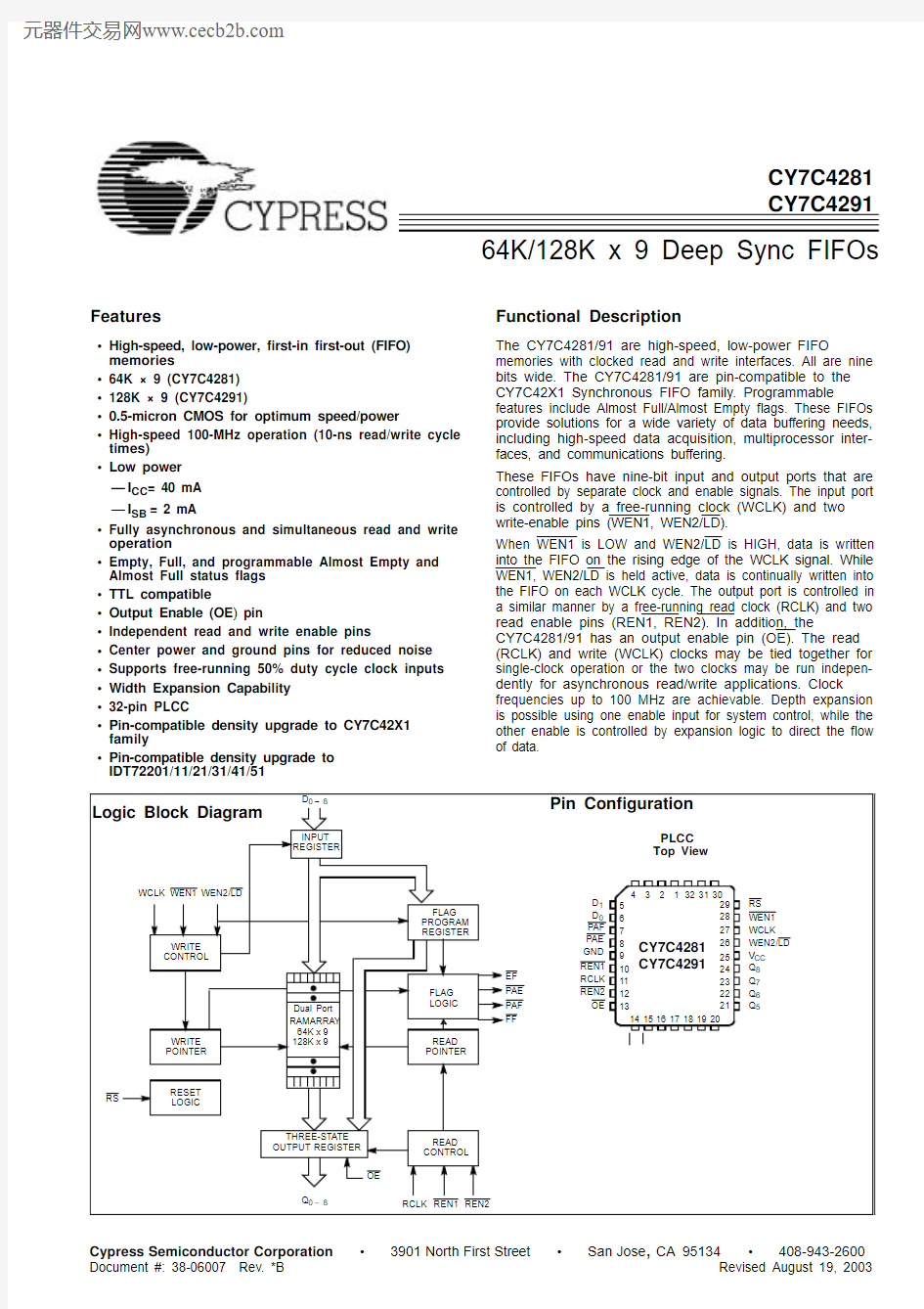
The CY7C4281/91 are high-speed, low-power FIFO memories with clocked read and write interfaces. All are nine bits wide. The CY7C4281/91 are pin-compatible to the CY7C42X1 Synchronous FIFO family. Programmable features include Almost Full/Almost Empty flags. These FIFOs provide solutions for a wide variety of data buffering needs,including high-speed data acquisition, multiprocessor inter-faces, and communications buffering.
These FIFOs have nine-bit input and output ports that are controlled by separate clock and enable signals. The input port is controlled by a free-running clock (WCLK) and two write-enable pins (WEN1, WEN2/LD).
When WEN1 is LOW and WEN2/LD is HIGH, data is written into the FIFO on the rising edge of the WCLK signal. While WEN1, WEN2/LD is held active, data is continually written into the FIFO on each WCLK cycle. The output port is controlled in a similar manner by a free-running read clock (RCLK) and two read enable pins (REN1, REN2). In addition, the CY7C4281/91 has an output enable pin (OE). The read (RCLK) and write (WCLK) clocks may be tied together for single-clock operation or the two clocks may be run indepen-dently for asynchronous read/write applications. Clock frequencies up to 100 MHz are achievable. Depth expansion is possible using one enable input for system control, while the other enable is controlled by expansion logic to direct the flow of data.
THREE-STATE OUTPUT REGISTER
READ CONTROL
FLAG LOGIC
WRITE CONTROL
WRITE POINTER
READ POINTER
RESET LOGIC
INPUT REGISTER
FLAG PROGRAM REGISTER
D 0?8
RCLK Q 0–8
WEN1WCLK RS
OE
Dual Port 64K x 9128K x 9
WEN2/LD
REN1REN2
EF
PAE PAF FF
RAMARRAY Logic Block Diagram
Pin Configuration
PLCC D 1D 0RCLK V CC D 8D 7
D 6
D 5
D 4
D 3
GND WCLK WEN2/LD Q 8Q 7D 2
PAF PAE 5678910111213
REN1OE
REN243213130
3221
2223242728
292526
14 151617181920Q 6Q 5
WEN1RS F F Q 0
Q 1
Q 2
Q 3
Q 4
E F Top View
CY7C4281CY7C4291
CY7C4281
CY7C4291 Pin Definitions
Signal Name Description I/O Description
D0–8Data Inputs I Data Inputs for 9-bit bus.
Q0 ? 8Data Outputs O Data Outputs for 9-bit bus.
WEN1Write Enable 1I The only write enable when device is configured to have programmable flags.
Data is written on a LOW-to-HIGH transition of WCLK when WEN1 is asserted and FF
is HIGH. If the FIFO is configured to have two write enables, data is written on a
LOW-to-HIGH transition of WCLK when WEN1 is LOW and WEN2/LD and FF are HIGH. WEN2/LD
Dual Mode Pin
Write Enable 2I If HIGH at reset, this pin operates as a second write enable. If LOW at reset, this
pin operates as a control to write or read the programmable flag offsets. WEN1 must be
LOW and WEN2 must be HIGH to write data into the FIFO. Data will not be written into
the FIFO if the FF is LOW. If the FIFO is configured to have programmable flags,
WEN2/LD is held LOW to write or read the programmable flag offsets.
Load
REN1, REN2Read Enable
Inputs
I Enables the device for Read operation. Both REN1 and REN2 must be asserted to
allow a read operation.
WCLK Write Clock I The rising edge clocks data into the FIFO when WEN1 is LOW and WEN2/LD is
HIGH and the FIFO is not Full. When LD is asserted, WCLK writes data into the
programmable flag-offset register.
RCLK Read Clock I The rising edge clocks data out of the FIFO when REN1 and REN2 are LOW and
the FIFO is not Empty. When WEN2/LD is LOW, RCLK reads data out of the program-
mable flag-offset register.
EF Empty Flag O When EF is LOW, the FIFO is empty. EF is synchronized to RCLK.
FF Full Flag O When FF is LOW, the FIFO is full. FF is synchronized to WCLK.
PAE Programmable
Almost Empty
O When PAE is LOW, the FIFO is almost empty based on the almost empty offset
value programmed into the FIFO. PAE is synchronized to RCLK.
PAF Programmable
Almost Full
O When PAF is LOW, the FIFO is almost full based on the almost full offset value
programmed into the FIFO. PAF is synchronized to WCLK.
RS Reset I Resets device to empty condition. A reset is required before an initial read or write
operation after power-up.
OE Output Enable I When OE is LOW, the FIFO’s data outputs drive the bus to which they are
connected. If OE is HIGH, the FIFO’s outputs are in High Z (high-impedance) state.
CY7C4281CY7C4291
Density64k x 9128k x 9
Package32-pin PLCC32-pin PLCC
Selection Guide
7C4281/91-107C4281/91-157C4281/91-25Unit Maximum Frequency 10066.740MHz Maximum Access Time81015ns Minimum Cycle Time101525ns Minimum Data or Enable Set-up 346ns Minimum Data or Enable Hold 0.511ns Maximum Flag Delay81015ns Active Power Supply Current (I CC1)Commercial404040mA
Industrial45
CY7C4281
CY7C4291 Functional Description (continued)
The CY7C4281/91 provides four status pins: Empty, Full,
Programmable Almost Empty, and Programmable Almost Full.
The Almost Empty/Almost Full flags are programmable to
single-word granularity. The programmable flags default to
Empty+7 and Full-7.
The flags are synchronous, i.e., they change state relative to
either the read clock (RCLK) or the write clock (WCLK). When
entering or exiting the Empty and Almost Empty states, the
flags are updated exclusively by the RCLK. The flags denoting
Almost Full and Full states are updated exclusively by WCLK.
The synchronous flag architecture guarantees that the flags
maintain their status for at least one cycle.
All configurations are fabricated using an advanced 0.5μ
CMOS technology. Input ESD protection is greater than
2001V, and latch-up is prevented by the use of guard rings.
Architecture
The CY7C4281/91 consists of an array of 64K to 128K words
of nine bits each (implemented by a dual-port array of SRAM
cells), a read pointer, a write pointer, control signals (RCLK,
WCLK, REN1, REN2, WEN1, WEN2, RS), and flags (EF, PAE,
PAF, FF).
Resetting the FIFO
Upon power-up, the FIFO must be reset with a Reset (RS)
cycle. This causes the FIFO to enter the Empty condition
signified by EF being LOW. All data outputs (Q0–8) go LOW
t RSF after the rising edge of RS. In order for the FIFO to reset
to its default state, the user must not read or write while RS is
LOW. All flags are guaranteed to be valid t RSF after RS is taken
LOW.
FIFO Operation
When the WEN1 signal is active LOW, WEN2 is active HIGH,
and FF is active HIGH, data present on the D0–8 pins is written
into the FIFO on each rising edge of the WCLK signal.
Similarly, when the REN1 and REN2 signals are active LOW
and EF is active HIGH, data in the FIFO memory will be
presented on the Q0–8 outputs. New data will be presented on
each rising edge of RCLK while REN1 and REN2 are active.
REN1 and REN2 must set up t ENS before RCLK for it to be
a valid read function. WEN1 and WEN2 must occur t ENS
before WCLK for it to be a valid write function.
An output enable (OE) pin is provided to three-state the Q0–8
outputs when OE is asserted. When OE is enabled (LOW),
data in the output register will be available to the Q0–8 outputs
after t OE. If devices are cascaded, the OE function will only
output data on the FIFO that is read enabled.
The FIFO contains overflow circuitry to disallow additional
writes when the FIFO is full, and underflow circuitry to disallow
additional reads when the FIFO is empty. An empty FIFO
maintains the data of the last valid read on its Q0–8 outputs
even after additional reads occur.
Write Enable 1 (WEN1) — If the FIFO is configured for
programmable flags, Write Enable 1 (WEN1) is the only write
enable control pin. In this configuration, when Write Enable 1
(WEN1) is LOW, data can be loaded into the input register and
RAM array on the LOW-to-HIGH transition of every write clock
(WCLK). Data is stored is the RAM array sequentially and
independently of any on-going read operation.
Write Enable 2/Load (WEN2/LD) — This is a dual-purpose
pin. The FIFO is configured at Reset to have programmable
flags or to have two write enables, which allows for depth
expansion. If Write Enable 2/Load (WEN2/LD) is set active
HIGH at Reset (RS = LOW), this pin operates as a second
write enable pin.
If the FIFO is configured to have two write enables, when Write
Enable (WEN1) is LOW and Write Enable 2/Load (WEN2/LD)
is HIGH, data can be loaded into the input register and RAM
array on the LOW-to-HIGH transition of every write clock
(WCLK). Data is stored in the RAM array sequentially and
independently of any on-going read operation.
Programming
When WEN2/LD is held LOW during Reset, this pin is the load
(LD) enable for flag offset programming. In this configuration,
WEN2/LD can be used to access the four nine-bit offset
registers contained in the CY7C4281/4291 for writing or
reading data to these registers.
When the device is configured for programmable flags and
both WEN2/LD and WEN1 are LOW, the first LOW-to-HIGH
transition of WCLK writes data from the data inputs to the
empty offset least significant bit (LSB) register. The second,
third, and fourth LOW-to-HIGH transitions of WCLK store data
in the empty offset most significant bit (MSB) register, full offset
LSB register, and full offset MSB register, respectively, when
WEN2/LD and WEN1 are LOW. The fifth LOW-to-HIGH
transition of WCLK while WEN2/LD and WEN1 are LOW
writes data to the empty LSB register again. Figure1 shows
the registers sizes and default values for the various device
types.
Figure 1.Offset Register Location and Default Values
64K×9
80
80
80
Empty Offset(LSB)Reg.
Default Value=007h
Full Offset(LSB)Reg
Default Value=007h
(MSB)
7
7
7
80
80
80
80
Empty Offset(LSB)Reg.
Default Value=007h
Full Offset(LSB)Reg
Default Value=007h
(MSB)
(MSB)
7
7
128K×9
80
(MSB)
7
Default Value=000h
Default Value=000h
Default Value=000h
Default Value=000h
CY7C4281
CY7C4291 It is not necessary to write to all the offset registers at one time.
A subset of the offset registers can be written; then by bringing
the WEN2/LD input HIGH, the FIFO is returned to normal read
and write operation. The next time WEN2/LD is brought LOW,
a write operation stores data in the next offset register in
sequence.
The contents of the offset registers can be read to the data
outputs when WEN2/LD is LOW and both REN1 and REN2
are LOW. LOW-to-HIGH transitions of RCLK read register
contents to the data outputs. Writes and reads should not be
performed simultaneously on the offset registers.
Programmable Flag (PAE, PAF) Operation
Whether the flag offset registers are programmed as
described in Table1 or the default values are used, the
programmable almost-empty flag (PAE) and programmable
almost-full flag (PAF) states are determined by their corre-
sponding offset registers and the difference between the read
and write pointers.
The number formed by the empty offset least significant bit
register and empty offset most significant bit register is
referred to as n and determines the operation of PAE. PAF is
synchronized to the LOW-to-HIGH transition of RCLK by one
flip-flop and is LOW when the FIFO contains n or fewer unread
words. PAE is set HIGH by the LOW-to-HIGH transition of
RCLK when the FIFO contains (n + 1) or greater unread words.
The number formed by the full offset least significant bit
register and full offset most significant bit register is referred to
as m and determines the operation of PAF. PAE is synchro-
nized to the LOW-to-HIGH transition of WCLK by one flip-flop
and is set LOW when the number of unread words in the FIFO
is greater than or equal to CY7C4281 (64K-m) and CY7C4291
(128K-m). PAF is set HIGH by the LOW-to-HIGH transition of
WCLK when the number of available memory locations is
greater than m.
Width Expansion Configuration
Word width may be increased simply by connecting the corre-
sponding input controls signals of multiple devices. A
composite flag should be created for each of the end-point
status flags (EF and FF). The partial status flags (PAE and
Figure2 demon-
strates a 18-bit word width by using two CY7C42X1s. Any
word width can be attained by adding additional CY7C42X1s.
When the CY7C42X1 is in a Width Expansion Configuration,
the Read Enable (REN2) control input can be grounded (see
Figure2). In this configuration, the Write Enable 2/Load
as a control to load and read the programmable flag offsets.
Flag Operation
The CY7C4281/91 devices provide five flag pins to indicate
the condition of the FIFO contents. Empty, Full, P AE, and P AF
are synchronous.
Full Flag
The Full Flag (FF) will go LOW when the device is full. Write
operations are inhibited whenever FF is LOW regardless of the
state of WEN1 and WEN2/LD. FF is synchronized to WCLK,
i.e., it is exclusively updated by each rising edge of WCLK.
Empty Flag
The Empty Flag (EF) will go LOW when the device is empty.
Read operations are inhibited whenever EF is LOW,
to RCLK, i.e., it is exclusively updated by each rising edge of
RCLK.
Note:
1.The same selection sequence applies to reading from the registers. REN1 and REN2 are enabled and a read is performed on the LOW-to-HIGH transition of RCLK. Table 1.Writing the Offset Registers
LD WEN WCLK[1]Selection
00
01No Operation
10Write Into FIFO
11No Operation
Empty Offset (LSB)
Empty Offset (MSB)
Full Offset (LSB)
Full Offset (MSB)
Table 2.Status Flags
Number of Words in FIFO
FF PAF PAE EF
CY7C4281CY7C4291
00H H L L
1 to n[2] 1 to n[2]H H L H
(n+1) to (65536 ?(m+1))(n+1) to (131072?(m+1))H H H H
(65536 ? m)[3] to 65535131072 ? m)[3] to 131071H L H H
65536131072L L H H
CY7C4281
CY7C4291
Figure 2.Block Diagram of 64k x 9/128k x 9 Deep Sync FIFO Memory Used in a Width Expansion Configuration Notes:
2.n = Empty Offset (n = 7 default value).
3.m = Full Offset (m = 7 default value).
FF
FF EF EF
WRITECLOCK(WCLK)
WRITE ENABLE1(WEN1)
WRITE ENABLE2/LOAD
(WEN2/LD)
PROGRAMMABLE(PAF)
FULL FLAG(FF)#1
CY7C4281/91
9
18
DATAIN(D)
RESET(RS)
9
RESET(RS)
READ CLOCK(RCLK)
READ ENABLE1(REN1)
OUTPUT ENABLE(OE)
PROGRAMMABLE(PAE)
EMPTY FLAG(EF)#1
9
DATA OUT(Q)
918
Read Enable2(REN2)
CY7C4281/91
EMPTY FLAG(EF)#2 FULL FLAG(FF)#2
Read Enable2(REN2)
CY7C4281
CY7C4291 Maximum Ratings
(Above which the useful life may be impaired. For user guide-
lines, not tested.)
Storage Temperature .......................................?65°C to +150°C
Ambient Temperature with
Power Applied....................................................?55°C to +125°C
Supply Voltage to Ground Potential.................?0.5V to +7.0V
DC Voltage Applied to Outputs
in High-Z State............................................?0.5V to V CC + 0.5V
DC Input Voltage.......................................?0.5V to V CC + 0.5V
Output Current into Outputs (LOW).............................20 mA
Static Discharge Voltage...........................................> 2001V
(per MIL-STD-883, Method 3015)
Latch-up Current.....................................................> 200 mA
Note:
4.The voltage on any input or I/O pin cannot exceed the power pin during power-up.
5.T A is the “instant on” case temperature.
6.Input signals switch from 0V to 3V with a rise/fall time of less than 3 ns, clocks and clock enables switch at maximum frequency 20 MHz, while data inputs switch
at 10 MHz. Outputs are unloaded. Icc1(typical) = (20 mA + (freq – 20 MHz)*(0.7 mA/MHz)).
7.All inputs = V CC – 0.2V, except WCLK and RCLK (which are at frequency = 0 MHz). All outputs are unloaded.
8.Tested initially and after any design or process changes that may affect these parameters.
9.C L = 30 pF for all AC parameters except for t OHZ.
10.C L = 5 pF for t OHZ.
Operating Range[4]
Range Ambient Temperature V CC
Commercial0°C to +70°C 5V
± 10%
Industrial[5]?40°C to +85°C 5V
± 10% Electrical Characteristics Over the Operating Range
Parameter Description Test Conditions
7C42X1?107C42X1?157C42X1?25
Unit
Min.Max.Min.Max.Min.Max.
V OH Output HIGH Voltage V CC = Min., I OH = ?2.0 mA 2.4 2.4 2.4V
V OL Output LOW Voltage V CC = Min., I OL = 8.0 mA0.40.40.4V
V IH Input HIGH Voltage 2.0V CC 2.0V CC 2.0V CC V
V IL Input LOW Voltage?0.50.8?0.50.8?0.50.8V
I IX Input Leakage Current V CC = Max.?10+10?10+10?10+10μA I OZL
I OZH
Output OFF, High Z Current OE > V IH, V SS < V O< V CC?10+10?10+10?10+10μA I CC1[6]Active Power Supply Current Com’l404040mA
Ind454545mA I SB[7]Average Standby Current Com’l222mA
Ind2mA Capacitance[8]
Parameter Description Test Conditions Max.Unit
C IN Input Capacitance T A = 25°C, f = 1 MHz,
V CC = 5.0V
5pF
C OUT Output Capacitance7pF
AC Test Loads and Waveforms[9, 10]
3.0V
5V
OUTPUT
R11.1K?
R2
680?
C L
INCLUDING
JIG AND
SCOPE
GND
90%
10%
90%
10%
≤3ns≤3ns OUTPUT 1.91V
Equivalent to:THé VENIN EQUIVALENT
420?
ALL INPUT PULSES
CY7C4281
CY7C4291 Switching Characteristics Over the Operating Range
Parameter Description
7C42X1-107C42X1-157C42X1-25
Unit
Min.Max.Min.Max.Min.Max.
t S Clock Cycle Frequency10066.740MHz t A Data Access Time28210215ns t CLK Clock Cycle Time101525ns t CLKH Clock HIGH Time 4.5610ns t CLKL Clock LOW Time 4.5610ns t DS Data Set-up Time346ns t DH Data Hold Time0.511ns t ENS Enable Set-up Time346ns t ENH Enable Hold Time0.511ns t RS Reset Pulse Width[11]101525ns t RSS Reset Set-up Time81015ns t RSR Reset Recovery Time81015ns t RSF Reset to Flag and Output Time101525ns t OLZ Output Enable to Output in Low Z[12]000ns t OE Output Enable to Output Valid3738312ns t OHZ Output Enable to Output in High Z[12]3738312ns t WFF Write Clock to Full Flag81015ns t REF Read Clock to Empty Flag81015ns t PAF Clock to Programmable Almost-Full Flag81015ns t PAE Clock to Programmable Almost-Full Flag81015ns t SKEW1Skew Time between Read Clock and Write Clock for
Empty Flag and Full Flag
5610ns
t SKEW2Skew Time between Read Clock and Write Clock for
Almost-Empty Flag and Almost-Full Flag
101518ns
Notes:
11.Pulse widths less than minimum values are not allowed.
12.Values guaranteed by design, not currently tested.
CY7C4281
CY7C4291 Switching Waveforms
Notes:
13.t SKEW1 is the minimum time between a rising RCLK edge and a rising WCLK edge to guarantee that FF will go HIGH during the current clock cycle. If the time between the rising
edge of RCLK and the rising edge of WCLK is less than t SKEW1, then FF may not change state until the next WCLK rising edge.
14.t SKEW1 is the minimum time between a rising WCLK edge and a rising RCLK edge to guarantee that EF will go HIGH during the current clock cycle. It the time between the rising
edge of WCLK and the rising edge of RCLK is less than t SKEW2, then EF may not change state until the next RCLK rising edge.
Write Cycle Timing
t CLKH t CLKL
NO OPERATION
t DS
t SKEW1
t ENS
WEN1
t CLK
t DH
t WFF t WFF
t ENH
WCLK
D0–D17
FF
REN1, REN2
RCLK
NO OPERATION WEN2
(if applicable)
[13]
REN1, REN2
Read Cycle Timing
t CLKH t CLKL
NO OPERATION
t SKEW1
WEN1
t CKL
t OHZ
t REF
t REF
RCLK
Q0–Q17
EF
WCLK
OE
t OE
t ENS
t OLZ
t A
t ENH
VALID DATA
WEN2
[14]
CY7C4281
CY7C4291 Notes:
15.The clocks (RCLK, WCLK) can be free-running during reset.
16.After reset, the outputs will be LOW if OE = 0 and three-state if OE=1.
17.Holding WEN2/LD HIGH during reset will make the pin act as a second enable pin. Holding WEN2/LD LOW during reset will make the pin act as a load enable for the
programmable flag offset registers.
Switching Waveforms (continued)
Reset Timing
t RS
t RSR
Q0-Q8
RS
t RSF
t RSF
t RSF
O E=1
OE=0 REN1,
REN2
EF,PAE
FF,PAF
t RSS
t RSR
t RSS
t RSR
t RSS
WEN2/LD
WEN1
[15]
[17]
[16]
CY7C4281
CY7C4291 Notes:
18.When t SKEW1 > minimum specification, t FRL (maximum) = t CLK + t SKEW2. When t SKEW1 < minimum specification, t FRL (maximum) = either 2*t CLK + t SKEW1 or t CLK + t SKEW1.
The Latency Timing applies only at the Empty Boundary (EF = LOW).
19.The first word is available the cycle after EF goes HIGH, always.
Switching Waveforms (continued)
D0(FIRST VALID WRITE)
First Data Word Latency after Reset with Read and Write
t SKEW1
WEN1
WCLK
Q0–Q8
EF
REN1,
REN2
OE
t OE
t ENS
t OLZ
t DS
RCLK
t REF
t A
t FRL
D1D2D3D4
D0D1 D0–D8
t A
WEN2
(if applicable)
[18]
[19]
CY7C4281
CY7C4291 Switching Waveforms (continued)
DATA WRITE 2
DATA WRITE 1
t SKEW1
DATA IN OUTPUT REGISTER
Empty Flag Timing
WCLK
Q0–Q8
EF
REN1,
REN2
OE
t DS
RCLK
t REF
t A
t FRL
D0–D8
DATA READ
t SKEW2
t FRL
t REF
t DS
WEN2
(if applicable)
ENS
t REF
LOW
[18][18]
t ENS
WEN1
t ENH
t ENS
t ENH
t ENS t ENH t t ENH
CY7C4281
CY7C4291 Notes:
20.t SKEW2 is the minimum time between a rising WCLK and a rising RCLK edge for PAE to change state during that clock cycle. If the time between the edge of WCLK and the rising
RCLK is less than t SKEW2, then P AE may not change state until the next RCLK.
21.PAE offset = n.
22.If a read is preformed on this rising edge of the read clock, there will be Empty + (n?1) words in the FIFO when PAE goes LOW.
Switching Waveforms (continued)
Q0–Q8
REN1,
REN2
WEN1
WEN2
(if applicable)
D0–D8
NEXT DATA READ
DATA WRITE
NO WRITE
DATA IN OUTPUT REGISTER
Full Flag Timing
FF
WCLK
OE
RCLK
t A
DATA READ
t SKEW1t DS
t ENS
t ENH
t WFF
t A
t SKEW1
t ENS
t ENH
t WFF
DATA WRITE
NO WRITE
t WFF
LOW
[13][13]
t ENH
Programmable Almost Empty Flag Timing
WCLK
PAE
RCLK
t CLKH
t ENS
t CLKL
t ENS
t PAE
N+1WORDS
IN FIFO
t ENH
t ENS
t ENH
t ENS
t PAE
REN1,
REN2
WEN1
WEN2
(if applicable)
t SKEW2[20]
Note 21
Note 22
CY7C4281
CY7C4291 Notes:
23.If a write is performed on this rising edge of the write clock, there will be Full ? (m?1) words of the FIFO when PAF goes LOW.
24.PAF offset = m.
25.16,384 ? m words for CY7C4281, 32,768 ? m words for CY4291.
26.t SKEW2 is the minimum time between a rising RCLK edge and a rising WCLK edge for PAF to change during that clock cycle. If the time between the rising edge of RCLK and
the rising edge of WCLK is less than t SKEW2, then P AF may not change state until the next WCLK.
Switching Waveforms (continued)
t ENH
Programmable Almost Full Flag Timing
WCLK
PAF
RCLK
t CLKH
t ENS
(FULL ?M) WORDS
IN FIFO
t CLKL
t ENS
FULL ?(M+1)WORDS
IN FIFO
t ENH
t ENS
t ENH
t ENS
t PAF
REN1,
REN2
WEN1
WEN2
(if applicable)
t SKEW2t PAF
[25]
[26]
[23]
Note 24
t ENH
WriteProgrammable Registers
WEN2/LD
WCLK
t CLKH
t ENS
t CLKL
PAE OFFSET
LSB
D0–D8
WEN1
t ENS
PAF OFFSET
MSB
t CLK
t DS t DH
PAE OFFSET
MSB
PAF OFFSET
LSB
CY7C4281
CY7C4291 Switching Waveforms (continued)
PAF OFFSET
MSB
PAF OFFSET
LSB
t ENH
Read Programmable Registers
WEN2/LD
RCLK
t CLKH
t ENS
t CLKL
PAE OFFSET LSB
Q0–Q15
REN1,
REN2
t ENS
PAE OFFSET MSB
t CLK
UNKNOWN
t A
Ordering Information
64K x 9 Deep Sync FIFO
Speed
(ns)Ordering Code
Package
Name
Package
Type
Operating
Range 10CY7C4281-10JC J6532-Lead Plastic Leaded Chip Carrier Commercial CY7C4281-10JI J6532-Lead Plastic Leaded Chip Carrier Industrial 15CY7C4281-15JC J6532-Lead Plastic Leaded Chip Carrier Commercial 25CY7C4281-25JC J6532-Lead Plastic Leaded Chip Carrier Commercial 128K x 9 Deep Sync FIFO
Speed
(ns)Ordering Code
Package
Name
Package
Type
Operating
Range 10CY7C4291-10JC J6532-Lead Plastic Leaded Chip Carrier Commercial CY7C4291-10JI J6532-Lead Plastic Leaded Chip Carrier Industrial 15CY7C4291-15JC J6532-Lead Plastic Leaded Chip Carrier Commercial 25CY7C4291-25JC J6532-Lead Plastic Leaded Chip Carrier Commercial
CY7C4281
CY7C4291 Package Diagrams
All product and company names mentioned in this document are the trademarks of their respective holders.
32-Lead Plastic Leaded Chip Carrier J65
51-85002-*B
CY7C4281
CY7C4291 Document History Page
Document Title: CY7C4281, CY7C4291 64K/128K X 9 Deep Sync FIFOs
Document Number: 38-06007
REV.ECN NO.Issue Date
Orig. of
Change Description of Change **10646807/12/01SZV Change from Spec number: 38-00587 to 38-06007
*A12225912/26/02RBI Power up requirements added to Operating Range Information
*B12785408/22/03FSG Removed Preliminary
Fixed empty flag timing diagram
Switching waveform diagram typo fixed