MAX4331ESA+T中文资料

General Description
The MAX4330–MAX4334 single/dual/quad op amps combine a wide 3MHz bandwidth, low-power operation,and excellent DC accuracy with Rail-to-Rail ?inputs and outputs. These devices require only 245μA per amplifier,and operate from either a single +2.3V to +6.5V supply or dual ±1.15V to ±3.25V supplies. The input common-mode voltage range extends 250mV beyond V EE and V CC , and the outputs swing rail-to-rail. The MAX4331/MAX4333 feature a shutdown mode in which the output goes high impedance and the supply current decreases to 9μA per amplifier.
Low-power operation combined with rail-to-rail input common-mode range and output swing makes these amplifiers ideal for portable/battery-powered equipment and other low-voltage, single-supply applications.Although the minimum operating voltage is specified at 2.3V, these devices typically operate down to 2.0V. Low offset voltage and high speed make these amplifiers excellent choices for signal-conditioning stages in pre-cision, low-voltage data-acquisition systems. The MAX4330 is available in the space-saving 5-pin SOT23package, and the MAX4331/MAX4333 are offered in a μMAX package.
Applications
Portable/Battery-Powered Equipment Data-Acquisition Systems Signal Conditioning
Low-Power, Low-Voltage Applications
____________________________Features
o 3MHz Gain-Bandwidth Product o 245μA Quiescent Current per Amplifier o Available in Space-Saving SOT23-5 Package (MAX4330)o +2.3V to +6.5V Single-Supply Operation
o Rail-to-Rail Input Common-Mode Voltage Range o Rail-to-Rail Output Voltage Swing o 250μV Offset Voltage
o Low-Power, 9μA (per amp) Shutdown Mode (MAX4331/MAX4333)o No Phase Reversal for Overdriven Inputs o Capable of Driving 2k ?Loads o Unity-Gain Stable
MAX4330–MAX4334
Single/Dual/Quad, Low-Power, Single-Supply,
Rail-to-Rail I/O Op Amps with Shutdown
________________________________________________________________Maxim Integrated Products
1
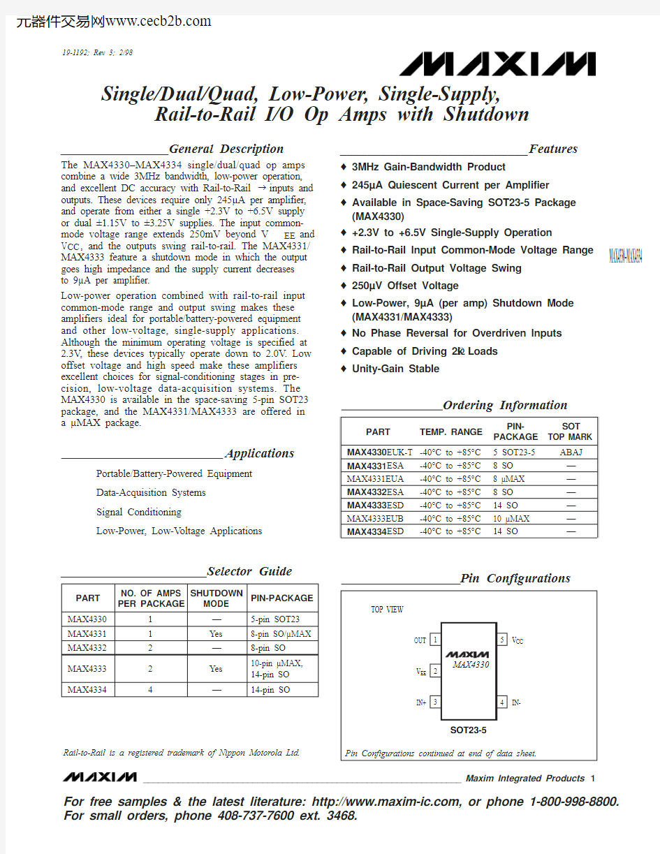
Pin Configurations
19-1192; Rev 3; 2/98
Selector Guide
Rail-to-Rail is a registered trademark of Nippon Motorola Ltd.For free samples & the latest literature: https://www.wendangku.net/doc/9f6545454.html,, or phone 1-800-998-8800.For small orders, phone 408-737-7600 ext. 3468.
M A X 4330–M A X 4334
Single/Dual/Quad, Low-Power, Single-Supply,Rail-to-Rail I/O Op Amps with Shutdown
ABSOLUTE MAXIMUM RATINGS
DC ELECTRICAL CHARACTERISTICS
(V = +2.3V to +6.5V, V = 0V, V = 0V, V = (V / 2), R tied to (V / 2), V SHDN = +25°C, unless otherwise noted.)
Stresses beyond those listed under “Absolute Maximum Ratings” may cause permanent damage to the device. These are stress ratings only, and functional operation of the device at these or any other conditions beyond those indicated in the operational sections of the specifications is not implied. Exposure to absolute maximum rating conditions for extended periods may affect device reliability.
Supply Voltage, V CC to V EE .....................................................7V IN_+, IN_-, SHDN Voltage................(V EE - 0.3V) to (V CC + 0.3V)Output Short-Circuit Duration....................................Continuous
(short to either supply)
Continuous Power Dissipation (T A = +70°C)
5-Pin SOT23 (derate 7.1mW/°C above +70°C).............571mW 8-Pin SO (derate 5.88mW/°C above +70°C).................471mW 8-Pin μMAX (derate 4.10mW/°C above +70°C)............330mW
10-Pin μMAX (derate 5.60mW/°C above +70°C)..........444mW 14-Pin SO (derate 8.33mW/°C above +70°C)...............667mW Operating Temperature Ranges
MAX433_C/D .......................................................0°C to +70°C MAX433_E_ _....................................................-40°C to +85°C Maximum Junction Temperature.....................................+150°C Storage Temperature Range.............................-65°C to +160°C Lead Temperature (soldering, 10sec).............................+300°C
MAX4330–MAX4334 Single/Dual/Quad, Low-Power, Single-Supply, Rail-to-Rail I/O Op Amps with Shutdown
_______________________________________________________________________________________3
DC ELECTRICAL CHARACTERISTICS (continued)
(V CC= +2.3V to +6.5V, V EE= 0V, V CM= 0V, V OUT= (V CC/ 2), R L tied to (V CC/ 2), V SHDN≥2V, T A= +25°C, unless otherwise noted.)
DC ELECTRICAL CHARACTERISTICS
(V CC= +2.3V to +6.5V, V EE= 0V, V CM= 0V, V OUT= (V CC/ 2), R L tied to (V CC/ 2), V SHDN≥2V, T A= -40°C to +85°C,unless
otherwise noted.)
M A X 4330–M A X 4334
Single/Dual/Quad, Low-Power, Single-Supply,Rail-to-Rail I/O Op Amps with Shutdown 4_______________________________________________________________________________________
DC ELECTRICAL CHARACTERISTICS (continued)
(V CC = +2.3V to +6.5V, V EE = 0V, V CM = 0V, V OUT = (V CC / 2), R L tied to (V CC / 2), V SHDN ≥2V, T A = -40°C to +85°C,unless otherwise noted.)
Note 1:SHDN logic thresholds are referenced to V EE .
Note 2:The MAX4330EUK is 100% tested at T A = +25°C. All temperature limits are guaranteed by design.
MAX4330–MAX4334
Single/Dual/Quad, Low-Power, Single-Supply,
Rail-to-Rail I/O Op Amps with Shutdown
_______________________________________________________________________________________5
AC ELECTRICAL CHARACTERISTICS
(V CC = +5V, V EE = 0V, V CM = 0V, V OUT = (V CC / 2), R L = 10k ?to (V CC / 2), V SHDN ≥2V, C L = 15pF, T A = +25°C,unless otherwise noted.)
60-20100
1k
100k
10M
GAIN AND PHASE vs. FREQUENCY (NO LOAD)
FREQUENCY (Hz)G A I N (d B )P H A S E (D E G R E E S )
10k
1M
100M 50403020100-10180
-180********-45-90-135
60
-40100
1k 100k 10M
GAIN AND PHASE
FREQUENCY (Hz)G A I N (d B )
P H A S E (D E G R E E S )
10k 1M 100M 40
20
-20180
-180108
36
-36-108144720
-72
-144
-100
10
10010k 1M 10M POWER-SUPPLY REJECTION RATIO
FREQUENCY (Hz)
P S R R (d B )
1k 100k 100M
-20
-40
-60
-80
__________________________________________Typical Operating Characteristics
(V CC = +5V, V EE = 0V, V CM = V CC / 2, V SHDN > 2V, T A = +25°C, unless otherwise noted.)
M A X 4330–M A X 4334
Single/Dual/Quad, Low-Power, Single-Supply,Rail-to-Rail I/O Op Amps with Shutdown 6_______________________________________________________________________________________
-40
-20-30100-1040302050
-40
20
-20
40
60
80
100
INPUT BIAS CURRENT vs. TEMPERATURE
TEMPERATURE (°C)
I N P U T B I A S C U R R E N T (n A )
250
200150
100
50
TEMPERATURE (°C)
-20
-40-60
2006080
40100
OUTPUT SWING HIGH V C C - V O U T (m V )
120
100804020600
TEMPERATURE (°C)
-200-60-4020406080100
OUTPUT SWING LOW vs. TEMPERATURE
V O U T - V E E (m V )
1k
0.01
100
1k
100k 10M
OUTPUT IMPEDANCE vs. FREQUENCY
FREQUENCY (Hz)
O U T P U T I M P E D A N C E (?)
10k 1M 100M
100
101
0.11200
10008004000200600-200
TEMPERATURE (°C)
-40-200-6020406080100
OUTPUT LEAKAGE CURRENT
O U T P U T L E A K A G E C U R R E N T (p A
)
350
310330250270290210
190170
230150
TEMPERATURE (°C)
-20
-60
20
60
100
-4040
80SUPPLY CURRENT vs. TEMPERATURE
I C C (μA )
25
2015
10
5
TEMPERATURE (°C)
-40-60-20
40
60
80
20
100
SHUTDOWN SUPPLY CURRENT
vs. TEMPERATURE
I C C (μA
)
1500
50001000-500
-1000-1500
TEMPERATURE (°C)
-40-20
0-6020406080100
INPUT OFFSET VOLTAGE vs. TEMPERATURE
I N P U T O F F S E T V
O L T A G E (μV )
-30
-10-20100302040
02314567
INPUT BIAS CURRENT vs. COMMON-MODE VOLTAGE
COMMON-MODE VOLTAGE (V)
I N P U T B I A S C U R R E N T (n A )
____________________________Typical Operating Characteristics (continued)
(V CC = +5V, V EE = 0V, V CM = V CC / 2, V SHDN > 2V, T A = +25°C, unless otherwise noted.)
MAX4330–MAX4334
Single/Dual/Quad, Low-Power, Single-Supply,
Rail-to-Rail I/O Op Amps with Shutdown
_______________________________________________________________________________________7
____________________________Typical Operating Characteristics (continued)
(V CC = +5V, V EE = 0V, V CM = V CC / 2, V SHDN > 2V, T A = +25°C, unless otherwise noted.)
118
1081131039383889878
OUTPUT VOLTAGE: EITHER SUPPLY (V)0.100.20.30.50.40.6LARGE-SIGNAL GAIN vs. OUTPUT VOLTAGE (V = 2.3V, R TO V )
G A I N (d B )
-60-70-80
-90-110-130-120-100-140
TEMPERATURE (°C)
-20
-40-6002080
6040100
COMMON-MODE REJECTION
C O M M O N -M O
D
E R E J E C T I O N (d B )
115
105110
100
959085
TEMPERATURE (°C)
-40-60-20
06080
4020100
LARGE-SIGNAL GAIN
vs. TEMPERATURE (R = 2k ?)
G A I N (d B )
118
11411010698
909410286
OUTPUT VOLTAGE: EITHER SUPPLY (V)
0.100.20.50.40.30.6
LARGE-SIGNAL GAIN vs. OUTPUT VOLTAGE (V CC = 2.3V, R L TO V EE )
G A I N (d B
)
130
120125115105
9510011090
OUTPUT VOLTAGE: EITHER SUPPLY (V)
0.100.20.30.50.40.6
LARGE-SIGNAL GAIN vs. OUTPUT VOLTAGE (V CC = 6.5V, R L TO V EE )
G A I N (d B
)
140
1301201009011080
OUTPUT VOLTAGE: EITHER SUPPLY (V)0
0.1
0.2
0.30.40.50.6LARGE-SIGNAL GAIN vs. OUTPUT VOLTAGE (V CC = 6.5V, R L TO V CC )
G A I N (d B )
130
125120
115
110
TEMPERATURE (°C)
-40-60-20
60
80
40
20
100
LARGE-SIGNAL GAIN
vs. TEMPERATURE (R = 100k ?)
G A I N (d B )
2.00
1.951.901.851.801.75
1.701.65
1.60
M A X 4330/34-T O C 18
TEMPERATURE (°C)
-40-60-20
60
80
40
20
100
MINIMUM OPERATING VOLTAGE
vs. TEMPERATURE
V C C (V )
1
0.001
1
1k
10k
100k
TOTAL HARMONIC DISTORTION AND NOISE vs. FREQUENCY
0.01
0.1
FREQUENCY (Hz)
T H D + N O I S E (%)
100
10
M A X 4330–M A X 4334
Single/Dual/Quad, Low-Power, Single-Supply,Rail-to-Rail I/O Op Amps with Shutdown 8
_______________________________________________________________________________________
1
0.001
4.0
5.0
TOTAL HARMONIC DISTORTION AND NOISE vs. PEAK-TO-PEAK
SIGNAL AMPLITUDE
0.01
0.1
PEAK-TO-PEAK SIGNAL AMPLITUDE (V)
T H D + N O I S E (%)
4.6
4.8
4.2
4.4
80
100901201101301401
10
1001000
10000
CROSSTALK vs. FREQUENCY
M A X 4330/34-T O C 22
FREQUENCY (kHz)
C R O S S T A L K (d B )
10
200
6001000
CAPACITIVE LOAD STABILITY
8LOAD CAPACITANCE (pF)
L O A D R E S I S T A N C E (k ?)
400800
6
4
2
LARGE-SIGNAL TRANSIENT RESPONSE
(NONINVERTING)
MAX4330/34-TOC24
TIME (5μs/div)IN
OUT
V O L T A G E (2V /d i v )
A V = -1
IN
OUT
SMALL-SIGNAL TRANSIENT RESPONSE
(INVERTING)
MAX4330/34-TOC23
TIME (200ns/div)
V O L T A G E (50m V /d i v )
LARGE-SIGNAL TRANSIENT RESPONSE
(INVERTING)
MAX4330/34-TOC25
TIME (5μs/div)
IN
OUT
V O L T A G E (2V /d i v )
A V = +1
IN
OUT SMALL-SIGNAL TRANSIENT RESPONSE
(NONINVERTING)
MAX4330/34-TOC22
TIME (200ns/div)
V O L T A G E (50m V /d i v )
____________________________Typical Operating Characteristics (continued)
(V CC = +5V, V EE = 0V, V CM = V CC / 2, V SHDN > 2V, T A = +25°C, unless otherwise noted.)
MAX4330–MAX4334
Single/Dual/Quad, Low-Power, Single-Supply,
Rail-to-Rail I/O Op Amps with Shutdown
_______________________________________________________________________________________9
Pin Description
M A X 4330–M A X 4334
Single/Dual/Quad, Low-Power, Single-Supply,Rail-to-Rail I/O Op Amps with Shutdown 10______________________________________________________________________________________
_______________Detailed Description
Rail-to-Rail Input Stage
The MAX4330–MAX4334 have rail-to-rail input and out-put stages that are specifically designed for low-voltage, single-supply operation. The input stage con-sists of separate NPN and PNP differential stages,which operate together to provide a common-mode range extending to 0.25V beyond both supply rails. The crossover region, which occurs halfway between V CC and V EE , is extended to minimize degradation in CMRR caused by mismatched input pairs. The input offset volt-age is typically 250μV. Low offset voltage, high band-width, rail-to-rail common-mode input range, and rail-to-rail outputs make this family of op amps an excel-lent choice for precision, low-voltage data-acquisition systems.
Since the input stage consists of NPN and PNP pairs,the input bias current changes polarity as the input volt-age passes through the crossover region. Match the effective impedance seen by each input to reduce the offset error due to input bias currents flowing through external source impedances (Figures 1a and 1b). The combination of high source impedance with input capacitance (amplifier input capacitance plus stray capacitance) creates a parasitic pole that produces an underdamped signal response. Reducing input capaci-tance or placing a small capacitor across the feedback resistor improves response.
The MAX4330–MAX4334’s inputs are protected from large differential input voltages by internal 1k ?series resistors and back-to-back triple diode stacks across the inputs (Figure 2). For differential input voltages (much less than 1.8V), input resistance is typically 2.3M ?. For differential input voltages greater than 1.8V,input resistance is around 2k ?, and the input bias cur-rent can be approximated by the following equation:
I BIAS = (V DIFF - 1.8V) / 2k ?
In the region where the differential input voltage approaches 1.8V, input resistance decreases exponen-tially from 2.3M ?to 2k ?as the diode block begins con-ducting. Inversely, the bias current increases with the same curve.
Figure 1a. Reducing Offset Error Due to Bias Current (Noninverting)
Figure 1b. Reducing Offset Error Due to Bias Current (Inverting)
MAX4330–MAX4334
Single/Dual/Quad, Low-Power, Single-Supply,
Rail-to-Rail I/O Op Amps with Shutdown
______________________________________________________________________________________
11
Rail-to-Rail Output Stage
The MAX4330–MAX4334 output stage can drive up to a 2k ?load and still typically swing within 125mV of the rails. Figure 3 shows the output voltage swing of a MAX4331 configured as a unity-gain buffer. The operat-ing voltage is a single +3V supply, and the input volt-age is 3Vp-p. The output swings to within 70mV of V EE and 100mV of V CC , even with the maximum load applied (2k ?to mid-supply).
Driving a capacitive load can cause instability in many op amps, especially those with low quiescent current.The MAX4330–MAX4334 are stable for capacitive loads up to 150pF. The Capacitive Load Stability graph in the Typical Operating Characteristics gives the stable operating region for capacitive vs. resistive loads.Figures 4 and 5 show the response of the MAX4331with an excessive capacitive load, compared with the response when a series resistor is added between the output and the capacitive load. The resistor improves the circuit’s response by isolating the load capacitance from the op amp’s output (Figure 6).
Figure 2. Input Protection Circuit
Figure 3. Rail-to-Rail Input/Output Voltage Range
IN
1V/div
1V/div
OUT
20μs/div
V CC = 3V, R L = 2k ? TO V CC / 2
Figure 4. Small-Signal Transient Response with Excessive Capacitive Load
IN
50mV/div
50mV/div
OUT
2μs/div
R ISO = 0?, A V = +1 C L = 510pF V CC = 3V, R L = 100k ?
M A X 4330–M A X 4334
Single/Dual/Quad, Low-Power, Single-Supply,Rail-to-Rail I/O Op Amps with Shutdown 12______________________________________________________________________________________
__________Applications Information
Power-Up
The MAX4330–MAX4334 outputs typically settle within 5μs after power-up. Using the test circuit of Figure 7,Figures 8 and 9 show the output voltage and supply current on power-up and power-down.
Shutdown Mode
The MAX4331/MAX4333 feature a low-power shutdown mode. When the shutdown pin (SHDN ) is pulled low, the supply current drops to 9μA per amplifier (typical), the amplifier is disabled, and the outputs enter a high-impedance state. Pulling SHDN high or leaving it float-ing enables the amplifier. Figures 10 and 11 show the MAX4331/MAX4333’s output voltage and supply-current responses to a shutdown pulse.
Figure 5. Small-Signal Transient Response with Excessive Load and Isolation Resistor
IN
50mV/div
50mV/div
OUT 2μs/div
A V = +1, C L = 510pF R ISO = 39?Figure 7. Power-Up/Shutdown Test Circuit SHDN
0V TO +2.7V STEP FOR SHUTDOWN TEST
0V TO +2.7V STEP FOR POWER-UP TEST, +2.7V STEP FOR SHUTDOWN-ENABLE TEST
SUPPLY-CURRENT V CC
100?
2k 2k
Figure 8. Power-Up/Down Output Voltage
1V/div
500mV/div
5μs/div
MAX4330–MAX4334
Single/Dual/Quad, Low-Power, Single-Supply,
Rail-to-Rail I/O Op Amps with Shutdown
______________________________________________________________________________________13
Do not three-state SHDN . Due to the output leakage currents of three-state devices and the small internal pull-up current for SHDN , three-stating this pin could result in indeterminate logic levels, and could adversely affect op-amp operation.
The logic threshold for SHDN is always referred to V EE ,not GND. When using dual supplies, pull SHDN to V EE to place the op amp in shutdown mode.
Power Supplies and Layout
The MAX4330–MAX4334 operate from a single +2.3V to +6.5V power supply, or from dual ±1.15V to ±3.25V supplies. For single-supply operation, bypass the power supply with a 0.1μF capacitor to ground (V EE ).For dual supplies, bypass both V CC and V EE with their own set of capacitors to ground.
Good layout technique helps optimize performance by decreasing the amount of stray capacitance at the op amp’s inputs and outputs. To decrease stray capaci-tance, minimize trace lengths by placing external com-ponents close to the op amp’s pins.
Figure 9. Power-Up/Down Supply Current CC
1V/div
100CC
5μs/div
Figure 11. Shutdown Enable/Disable Supply Current
SHDN 1V/div
100CC
5μs/div
Figure 10. Shutdown Output Voltage Enable/Disable
SHDN 1V/div
500mV/div
5μs/div
M A X 4330–M A X 4334
Single/Dual/Quad, Low-Power, Single-Supply,Rail-to-Rail I/O Op Amps with Shutdown 14______________________________________________________________________________________
Pin Configurations (continued)
MAX4330–MAX4334
Single/Dual/Quad, Low-Power, Single-Supply,
Rail-to-Rail I/O Op Amps with Shutdown
______________________________________________________________________________________15
Tape-and-Reel Information
Chip Information
MAX4330/MAX4331
TRANSISTOR COUNT: 199
SUBSTRATE CONNECTED TO V EE MAX4332/MAX4333
TRANSISTOR COUNT: 398
SUBSTRATE CONNECTED TO V EE MAX4334
TRANSISTOR COUNT: 796
SUBSTRATE CONNECTED TO V EE
M A X 4330–M A X 4334
Single/Dual/Quad, Low-Power, Single-Supply,Rail-to-Rail I/O Op Amps with Shutdown
________________________________________________________Package Information
Maxim cannot assume responsibility for use of any circuitry other than circuitry entirely embodied in a Maxim product. No circuit patent licenses are implied. Maxim reserves the right to change the circuitry and specifications without notice at any time.
16____________________Maxim Integrated Products, 120 San Gabriel Drive, Sunnyvale, CA 94086 408-737-7600?1998 Maxim Integrated Products
Printed USA
is a registered trademark of Maxim Integrated Products.