HE8550-D-T92-B中文资料

UNISONIC TECHNOLOGIES CO., LTD
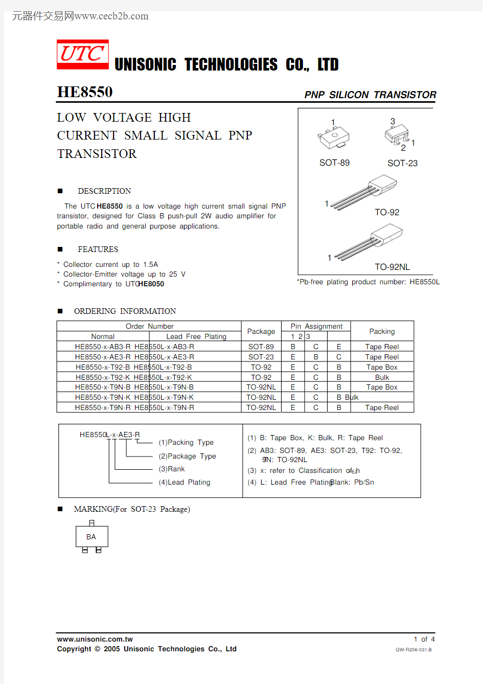
HE8550
PNP SILICON TRANSISTOR
LOW VOLTAGE HIGH
CURRENT SMALL SIGNAL PNP TRANSISTOR
DESCRIPTION
The UTC HE8550 is a low voltage high current small signal PNP transistor, designed for Class B push-pull 2W audio amplifier for portable radio and general purpose applications.
FEATURES
* Collector current up to 1.5A
* Collector-Emitter voltage up to 25 V * Complimentary to UTC HE8050
*Pb-free plating product number: HE8550L
ORDERING INFORMATION
Order Number Pin Assignment
Normal Lead Free Plating Package 1 2 3 Packing
HE8550-x-AB3-R HE8550L-x-AB3-R SOT-89 B C E Tape
Reel HE8550-x-AE3-R HE8550L-x-AE3-R SOT-23 E B C Tape Reel HE8550-x-T92-B HE8550L-x-T92-B TO-92 E C B Tape Box HE8550-x-T92-K HE8550L-x-T92-K TO-92 E C B Bulk HE8550-x-T9N-B HE8550L-x-T9N-B TO-92NL E C B Tape Box HE8550-x-T9N-K HE8550L-x-T9N-K TO-92NL E C B Bulk HE8550-x-T9N-R HE8550L-x-T9N-R TO-92NL E C B Tape Reel
MARKING(For SOT-23 Package)
ABSOLUTE MAXIMUM RATING (Ta=25℃, unless otherwise specified)
PARAMETER SYMBOL RATINGS UNIT
Collector-Base Voltage V CBO -40 V Collector-Emitter Voltage V CEO -25 V Emitter-Base Voltage V EBO -6 V
SOT-23 350 mW
SOT-89 0.5 W
Collector Dissipation (Ta=25) TO-92/TO-92NL P C 1 W
Collector Current I C -1.5 A Junction Temperature T J +150 Operating Ambient Temperature T OPR -40 ~ +150 Storage Temperature T STG -65 ~ +150
Note Absolute maximum ratings are those values beyond which the device could be permanently damaged.
Absolute maximum ratings are stress ratings only and functional device operation is not implied.
ELECTRICAL CHARACTERISTICS (Ta=25℃, unless otherwise specified)
PARAMETER SYMBOL
TEST CONDITIONS MIN TYP MAX UNIT
Collector-Base Breakdown Voltage BV CBO I C =-100μA, I E =0 -40 V Collector-Emitter Breakdown Voltage BV CEO I C =-2mA, I B =0 -25 V Emitter-Base Breakdown Voltage BV EBO I E =-100μA, I C =0 -6 V Collector Cut-Off Current I CBO V CB =-35V, I E =0 -100 nA Emitter Cut-Off Current I EBO
V EB =-6V, I C =0 -100 nA h FE1
V CE =-1V, I C =-5mA 45 170 h FE2
V CE =-1V, I C =-100mA 85 160 500 DC Current Gain h FE3
V CE =-1V, I C =-800mA 40 80 Collector-Emitter Saturation Voltage V CE(SAT)I C =-800mA, I B =-80mA -0.28 -0.5 V Base-Emitter Saturation Voltage V BE(SAT )I C =-800mA, I B =-80mA -0.98 -1.2 V Base-Emitter Voltage V BE V CE =-1V,I C =-10mA -0.66 -1.0 V Current Gain Bandwidth Product f T V CE =-10V,I C =-50mA 100 190 MHz Output Capacitance C ob
V CB =-10V, I E =0 f=1MHz 9.0 pF
CLASSIFICATION OF h FE2
RANK C D E
RANGE 120-200 160-300 250-500
TYPICAL CHARACTERISTICS
Static Characteristics
Collector -Emitter Voltage ( V)
C o l l e c t o r C u r r e n t , I C (m A )
Collector Current , I C (mA)
Base-Emitter on Voltage
C o l l e c t o r C u r r e n t
, I C (m A )
Base-Emitter Voltage (V)
-0.2-0.4-0.6-0.8-1.0
Collector Current , I C (mA)
Saturation Voltage -10-10-10-10
Current Gain-Bandwidth Product Collector Output Capacitance
Collector Current , I C (mA)
C u r r e n t G a i n -B a n d w i
d t h P r o d u c t ,f T (M H z )
Collector -Base Voltage (V)
10101010