A 115mW 12-BIT 50 MSPS PIPELINED ADC
A115mW12-BIT50MSPS PIPELINED ADC
Sumeet Mathur,Mrinal Das,Preetam Tadeparthy,Sourja Ray,Subhashish Mukherjee,
Dinakaran B.L.
Texas Instruments(India)
ABSTRACT
High sampling rate ADCs are needed in several communications applications like cable modems,and wireless LANs.In this paper we present a low power pipelined ADC cell implemented in a0.18um digital CMOS process.The ADC uses a4-bit/stage architecture for reduced power and area.The ADC has been put on a test chip to verify performance and achieves-70dB THD performance for10MHz input at50MHz sampling rate.
1.INTRODUCTION
Pipelined ADCs in several communication applications like cable modems and wireless LANs use higher than Nyquist sampling rates to relax requirement on the anti-alias filter driving the ADC.In this paper we present such a“12bit”ADC where the band of interest is0-10MHz but a sampling rate of50MHz has been chosen. The ADC has been designed as an analog cell in a digital dual supply voltage CMOS process for integration as part of more complex SOCs.
2.ADC ARCHITECTURE
Several pipelined ADC publications have been based on 1.5bit/stage designs[1][2].This is a popular choice because of its ease of design and the fact that it demands the inter-stage gain amplifiers operate at a nominal inter-stage gain of only2and are thus faster.However larger number of bits resolved in the first stage help improve linearity and also enable faster scaling of capacitors down the pipeline.A multi-bit architecture requires fewer inter stage amplifiers,which,in pipeline ADCs,especially at high speeds,consume bulk of the ADC power.Further increase in the number of bits per stage complicates the design of the sub-ADC or flash in each stage and also leads to increased load of comparators on the inter stage amplifier and sample and hold.For this design we chose 4-bits/stage design with16comparators in each flash so as to reduce the number of stages keeping the comparator design simple.The ADC architecture,shown in figure1, uses three stages of4bit/stage followed by a3-bit flash.
Figure1:ADC Architecture
3.DESIGN DESCRIPTION
3.1Design in Digital CMOS process
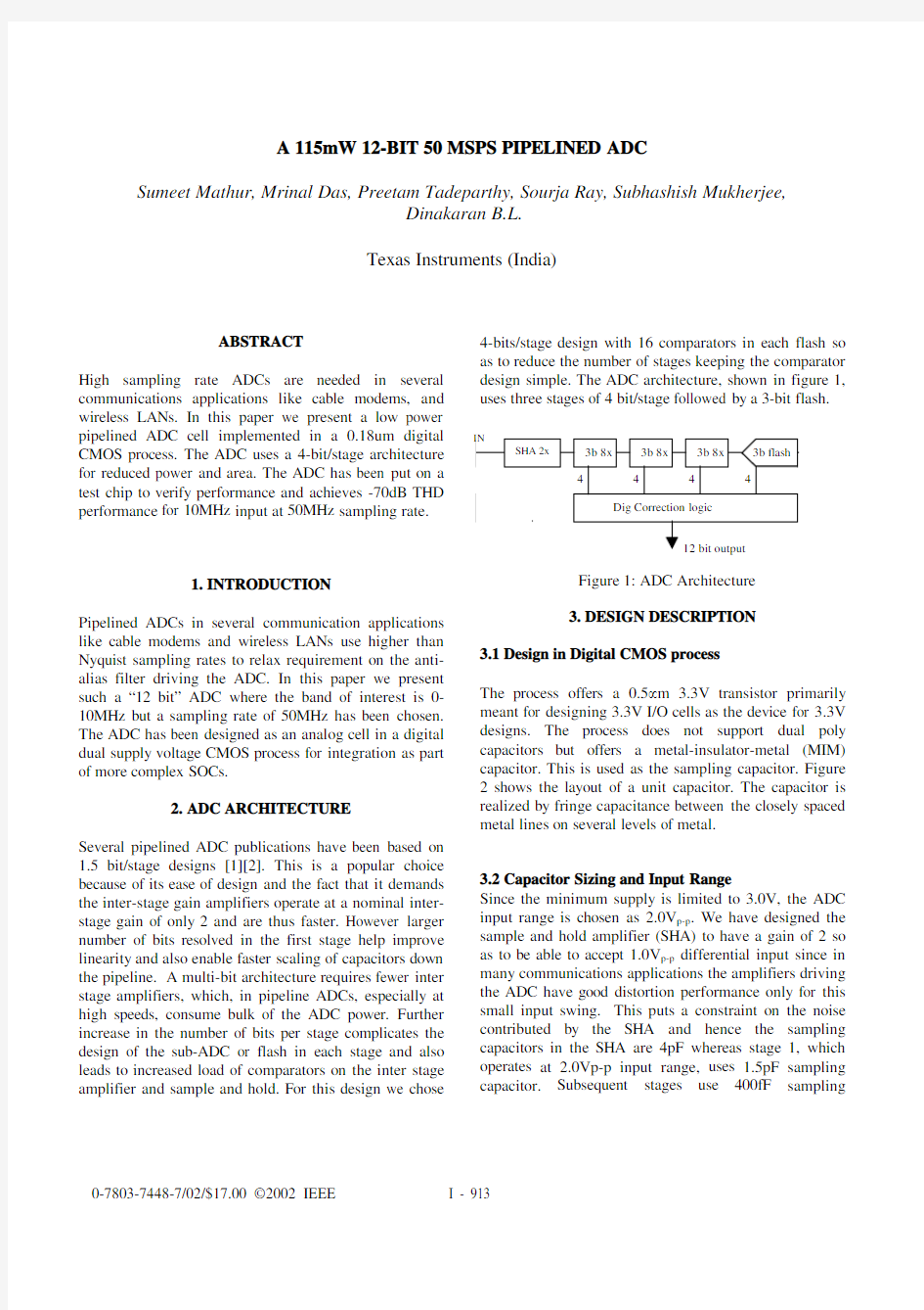
The process offers a0.5μm 3.3V transistor primarily meant for designing3.3V I/O cells as the device for3.3V designs.The process does not support dual poly capacitors but offers a metal-insulator-metal(MIM) capacitor.This is used as the sampling capacitor.Figure 2shows the layout of a unit capacitor.The capacitor is realized by fringe capacitance between the closely spaced metal lines on several levels of metal.
3.2Capacitor Sizing and Input Range
Since the minimum supply is limited to3.0V,the ADC input range is chosen as2.0V p-p.We have designed the sample and hold amplifier(SHA)to have a gain of2so as to be able to accept1.0V p-p differential input since in many communications applications the amplifiers driving the ADC have good distortion performance only for this small input swing.This puts a constraint on the noise contributed by the SHA and hence the sampling capacitors in the SHA are4pF whereas stage1,which operates at2.0Vp-p input range,uses1.5pF sampling capacitor.Subsequent stages use400fF sampling
capacitor.From a noise standpoint the capacitors in second stage do not need to be this large,we have chosen this size to keep the capacitors sufficiently larger than
parasitics.
Figure2:MIM Capacitor
3.2ADC Stage
The pipelined ADC stage consists of the switched capacitor gain stage,4-bit flash and the flash encoder to control the DAC switches.
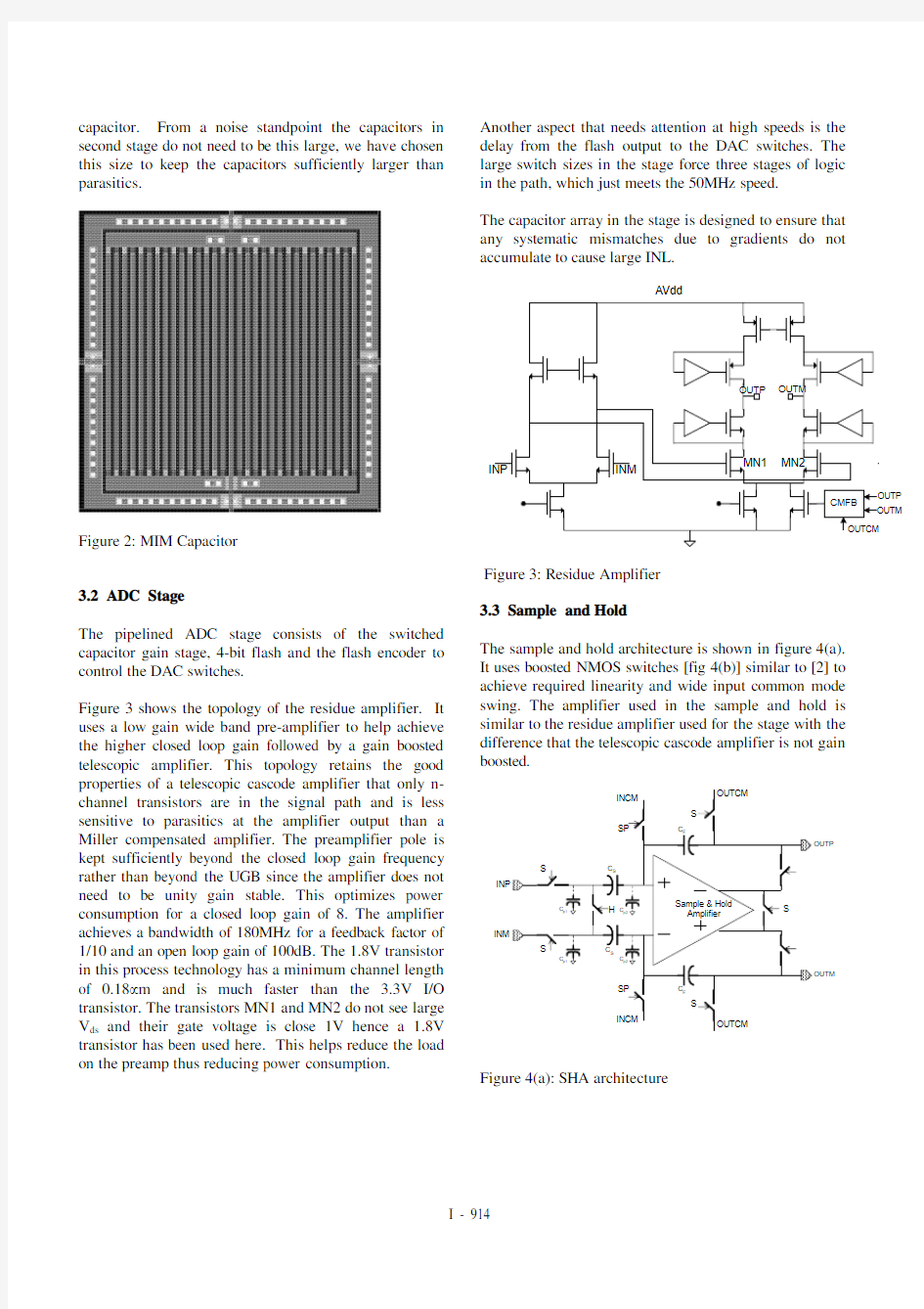
Figure3shows the topology of the residue amplifier.It uses a low gain wide band pre-amplifier to help achieve the higher closed loop gain followed by a gain boosted telescopic amplifier.This topology retains the good properties of a telescopic cascode amplifier that only n-channel transistors are in the signal path and is less sensitive to parasitics at the amplifier output than a Miller compensated amplifier.The preamplifier pole is kept sufficiently beyond the closed loop gain frequency rather than beyond the UGB since the amplifier does not need to be unity gain stable.This optimizes power consumption for a closed loop gain of8.The amplifier achieves a bandwidth of180MHz for a feedback factor of 1/10and an open loop gain of100dB.The1.8V transistor in this process technology has a minimum channel length of0.18μm and is much faster than the 3.3V I/O transistor.The transistors MN1and MN2do not see large V ds and their gate voltage is close1V hence a 1.8V transistor has been used here.This helps reduce the load on the preamp thus reducing power consumption.Another aspect that needs attention at high speeds is the delay from the flash output to the DAC switches.The large switch sizes in the stage force three stages of logic in the path,which just meets the50MHz speed.
The capacitor array in the stage is designed to ensure that any systematic mismatches due to gradients do not accumulate to cause large INL.
AVdd
Figure3:Residue Amplifier
3.3Sample and Hold
The sample and hold architecture is shown in figure4(a). It uses boosted NMOS switches[fig4(b)]similar to[2]to achieve required linearity and wide input common mode swing.The amplifier used in the sample and hold is similar to the residue amplifier used for the stage with the difference that the telescopic cascode amplifier is not gain boosted.
INM
Figure4(a):SHA architecture
Figure4(b):Voltage boost circuit for sampling switch 3.4Flash
Each stage in the ADC has a flash with16comparators. The comparator architecture chosen is a fully differential offset cancelled preamplifier followed by a latch.A switched capacitor network compares the inputs with the reference thresholds that are generated by a resistor-DAC.
An offset cancelled comparators scheme,shown in figure 5,senses the input referred offset of the preamplifier in the hold phase on the capacitors C S by putting the preamplifier in unity gain feedback
For the required performance the comparator input referred offset should be lesser than±62.5mV.The comparator was simulated for offset using process mismatch data and the TI Statistical design flow. Simulations show a worst case static offset within ±20mV.The comparator draws400μW of power.
REFP
INP
INM
REFM
Figure5:Offset cancelled comparator 3.5Clock Generator
The clock generator block generates the clock phases required for the ADC and SHA operation from the50 MHz system clock with the phase relationship shown in figure(Fig6).The clock is fed from the last stage upwards to ensure that a stage K is driving its output till just after stage K+1samples its inputs.The stringent timing requirements needed for operation at50MSPS is met by using the fast1.8V standard cell library gates in the main clock generation loop.The1.8V clocks are level-shifted to3.3V logic levels and cascaded buffers, which merely adds a constant delay in all the clock phases,drive the presented load with the required rise and fall times.The rising edges of pre-sample and sample are aligned using a feed-forward scheme that compensates for the reduction in the sampling time caused by skewing of these edges by unequal buffer chains in the clock paths clocks(similar technique is adopted for the hold clocks).
System
CLK
3.3V Buffers to drive switches
Figure6:The ADC clock generator
4.RESULTS
Figure7shows the die photograph of the ADC test-chip. In this process,to ensure sufficient metal density,dummy metals are added to the layout.Hence the die photo only shows top level metal geometries like the capacitors clearly.The INL/DNL plots of the ADC sampled at 50MHz and the FFT of the ADC output for a6MHz sine-wave sampled at50MHz are shown in figure8.Table I summarizes the results.
5.CONCLUSION
We have presented a multi bit pipeline ADC in a digital CMOS process.Multi bit designs reduce power and area as compared to1bit/stage designs as they require fewer inter-stage amplifiers and allow faster scaling of the pipeline.Future work can look at reducing the switch
M
M
1
SMPLZ_SEMIBOOST
sizes in the stage-sampling network as this forces the need for extra logic stage from the flash output to DAC controls and this limits the performance at higher conversion
rates.
Figure7:Die Photo of the ADC in the
test-chip. Figure8:INL,DNL and FFT for6MHz input
Table I:Summary of results
6.REFERENCES
[1]Sotoudeh Hanedi-Hagh,CAT Salama,“A10bit50 msamples low power pipelined A/D converter for cable modem applications,”ISCAS2001Vol1PP:424-427
[2]1Abo,A.M.;Gray,P.R.“A1.5-V,10-bit,14.3MS/s CMOS pipeline analog-to-digital converter”,IEEE JSSC,Vol:34,May1999,PP:599–606.
Resolution12BIT
SNR
(0-10MHz)band
68dB
THD-70dB
INL+/-2.1LSB
DNL<+/0.6LSB
Area 1.5SQMM
ADC Core Power
I/O Buffers
Int.Reference
115mW
40mW
21mW