M74HC4094中文资料
M54HC4094M74HC4094
February 1993
8BIT SIPO SHIFT LATCH REGISTER (3-STATE)
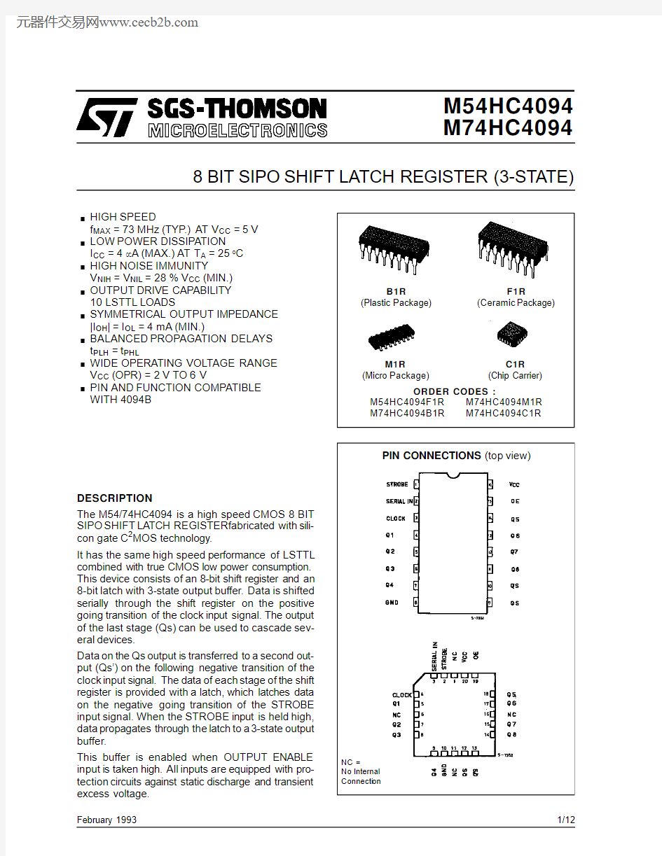
B1R
(Plastic Package)ORDER CODES :
M54HC4094F1R M74HC4094M1R M74HC4094B1R M74HC4094C1R
F1R
(Ceramic Package)
M1R
(Micro Package)C1R (Chip Carrier)
PIN CONNECTIONS (top view)
NC =
No Internal Connecti o n
DESCRIPTION
.HIGH SPEED
f MAX =73MHz (TYP.)AT V CC =5V .LOW POWER DISSIPATION I CC =4μA (MAX.)AT T A =25°C .HIGH NOISE IMMUNITY
V NIH =V NIL =28%V CC (MIN.).OUTPUT DRIVE CAPABILITY 10LSTTL LOADS
.SYMMETRICAL OUTPUT IMPEDANCE |I OH |=I OL =4mA (MIN.)
.BALANCED PROPAGATION DELAYS t PLH =t PHL
.WIDE OPERATING VOLTAGE RANGE V CC (OPR)=2V TO 6V
.
PIN AND FUNCTION COMPATIBLE WITH 4094B
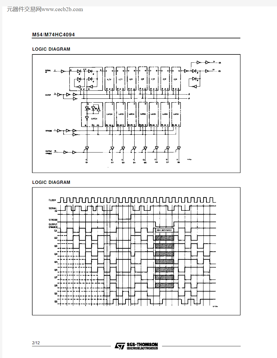
The M54/74HC4094is a high speed CMOS 8BIT SIPO SHIFT LATCH REGISTERfabricated with sili-con gate C 2MOS technology.
It has the same high speed performance of LSTTL combined with true CMOS low power consumption.This device consists of an 8-bit shift register and an 8-bit latch with 3-state output buffer.Data is shifted serially through the shift register on the positive going transition of the clock input signal.The output of the last stage (Qs)can be used to cascade sev-eral devices.
Data on the Qs output is transferred to a second out-put (Qs’)on the following negative transition of the clock input signal.The data of each stage of the shift register is provided with a latch,which latches data on the negative going transition of the STROBE input signal.When the STROBE input is held high,data propagates through the latch to a 3-state output buffer.
This buffer is enabled when OUTPUT ENABLE input is taken high.All inputs are equipped with pro-tection circuits against static discharge and transient excess voltage.
1/12
M54/M74HC4094 LOGIC DIAGRAM
LOGIC DIAGRAM 2/12
TRUTH TABLE
CK OE ST SI PARALLEL OUTPUT SERIAL OUTPUT Q1Qn Qs Qs’
H H L L Qn-1Q7NC
H H H H Qn-1Q7NC
H L X NC NC Q7NC
L X X Z Z Q7NC
H X X NC NC NC Qs
L X X Z Z NC Qs X:Don’t Care Z:High Impedance NC:No Change
PIN DESCRIPTION
PIN No SYMBOL NAME AND FUNCTION 1STROBE Strobe Input
2SERIAL IN Serial Input
3CLOCK Clock Input
4,5,6,7,
14,13,12,
11
Q1to Q7Parallel Outputs
9,10QS Q’S Serial Outputs
15OE Output Enable Input
8GND Ground(0V)
16V CC Positive Supply Voltage IEC LOGIC SYMBOL
INPUT AND OUTPUT EQUIVALENT CIRCUIT
M54/M74HC4094
3/12
ABSOLUTE MAXIMUM RATINGS
Symbol Parameter Value Unit V CC Supply Voltage-0.5to+7V V I DC Input Voltage-0.5to V CC+0.5V V O DC Output Voltage-0.5to V CC+0.5V
I IK DC Input Diode Current±20mA
I OK DC Output Diode Current±20mA
I O DC Output Source Sink Current Per Output Pin±25mA
I CC or I GND DC V CC or Ground Current±50mA
P D Power Dissipation500(*)mW T stg Storage Temperature-65to+150o C T L Lead Temperature(10sec)300o C Absolute Maximum Ratings are those values beyond whichdamage to the device may occu r.Functiona l ope ration und er these cond ition isnotimplied. (*)500mW:?65o C derate to300mW by10mW/o C:65o C to85o C
RECOMMENDED OPERATING CONDITIONS
Symbol Parameter Value Unit V CC Supply Voltage2to6V V I Input Voltage0to V CC V V O Output Voltage0to V CC V
T op Operating Temperature:M54HC Series
M74HC Series -55to+125
-40to+85
o C
o C
t r,t f Input Rise and Fall Time V CC=2V0to1000ns
V CC=4.5V0to500
V CC=6V0to400
M54/M74HC4094
4/12
DC SPECIFICATIONS
Symbol Parameter
Test Conditions Value
Unit V CC
(V)
T A=25o C
54HC and74HC
-40to85o C
74HC
-55to125o C
54HC
Min.Typ.Max.Min.Max.Min.Max.
V IH High Level Input
Voltage 2.0 1.5 1.5 1.5
V 4.5 3.15 3.15 3.15
6.0 4.2 4.2 4.2
V IL Low Level Input
Voltage 2.00.50.50.5
V 4.5 1.35 1.35 1.35
6.0 1.8 1.8 1.8
V OH High Level
Output Voltage 2.0
V I=
V IH
or
V IL
I O=-20μA
1.9
2.0 1.9 1.9
V 4.5 4.4 4.5 4.4 4.4
6.0 5.9 6.0 5.9 5.9
4.5I O=-4.0mA 4.18 4.31 4.13 4.10
6.0I O=-5.2mA 5.68 5.8 5.63 5.60
V OL Low Level Output
Voltage 2.0
V I=
V IH
or
V IL
I O=20μA
0.00.10.10.1
V 4.50.00.10.10.1
6.00.00.10.10.1
4.5I O=4.0mA0.170.260.370.40
6.0I O=5.2mA0.180.260.370.40
I I Input Leakage
Current 6.0
V I=V CC or GND±0.1±1±1μA
I OZ3State Output
Off State Current 6.0V I=V IH or V IL
V O=V CC or GND
±0.5±5.0±10μA
I CC Quiescent Supply
Current 6.0V I=V CC or GND44080μA
M54/M74HC4094
5/12
AC ELECTRICAL CHARACTERISTICS(C L=50pF,Input t r=t f=6ns)
Symbol Parameter
Test Conditions Value
Unit V CC
(V)
T A=25o C
54HC and74HC
-40to85o C
74HC
-55to125o C
54HC
Min.Typ.Max.Min.Max.Min.Max.
t TLH t THL Output Transition
Time
2.0307595110
ns
4.58151922
6.07131619
t PLH t PHL Propagation
Delay Time
(CLOCK-Qn)
2.092200250300
ns
4.526405060
6.020344351
t PLH t PHL Propagation
Delay Time
(C LOC K-QS,Q’S)
2.065150190225
ns
4.519303845
6.015263238
t PLH t PHL Propagation
Delay Time
(STROBE-Qn)
2.0751********
ns
4.520324048
6.016273441
t PZL t PZH 3State Output
Enable Time
2.058150190225
ns
4.516303845
6.013263238
t PHZ t PLZ 3State Output
Disable Time
2.0351********
ns
4.516303845
6.013263238
f MAX Maximum Clock
Frequency 2.0616 4.84
MHz 4.530662420
6.035802824
t W(H) t W(L)Minimum Pulse
Width
2.0177595110
ns
4.57151922
6.06131619
t W(L)Minimum Pulse
Width 2.028*******
ns 4.56151922
6.06131619
t s Minimum Set-up
Time
(SI)2.0307595110
ns 4.57151922
6.05131619
t s Minimum Set-up
Time
(ST)2.0451********
ns 4.510202529
6.08172125
t h Minimum Hold
Time
(SI,ST)2.0000
ns 4.5000
6.0000
C IN Input Capacitance5101010pF
C PD(*)Power Dissipation
Capacitance 140
pF
(*)C PD is defined as the value of the IC’s internal equivalent capac itanc e which is calculated from the operating current con sump tion without load. (Refer to Test Circuit).Average operting current can be obtained by the following equ ation.I CC(opr)=C PD?V CC?f IN+I CC/2(per FLIP/FLOP)
M54/M74HC4094
6/12
TEST WAVEFORM I CC (Opr.)SWITCHING CHARACTERISTICS TEST WAVEFORM
C P
D CALCULATION
C P
D is to be calculated with the following for-mula by using the measured value of I CC (Opr.)in the test circuit opposite.
C P
D =
I CC (Opr )f IN ×V CC In determining the typical value of C PD ,a relatively high frequency of 1MHz was ap-plied to f IN ,in order to eliminate any error caused by the quiescent supply current.
M54/M74HC4094
7/12
M54/M74HC4094
Plastic DIP16(0.25)MECHANICAL DATA
mm inch DIM.
MIN.TYP.MAX.MIN.TYP.MAX.
a10.510.020
B0.77 1.650.0300.065 b0.50.020
b10.250.010
D200.787 E8.50.335
e 2.540.100
e317.780.700
F7.10.280
I 5.10.201
L 3.30.130
Z 1.270.050
P001C 8/12
M54/M74HC4094 Ceramic DIP16/1MECHANICAL DATA
mm inch
DIM.
MIN.TYP.MAX.MIN.TYP.MAX.
A200.787
B70.276
D 3.30.130
E0.380.015
e317.780.700
F 2.29 2.790.0900.110
G0.40.550.0160.022
H 1.17 1.520.0460.060
L0.220.310.0090.012
M0.51 1.270.0200.050
N10.30.406
P7.88.050.3070.317
Q 5.080.200
P053D
9/12
M54/M74HC4094
SO16(Narrow)MECHANICAL DATA
mm inch DIM.
MIN.TYP.MAX.MIN.TYP.MAX.
A 1.750.068
a10.10.20.0040.007 a2 1.650.064 b0.350.460.0130.018 b10.190.250.0070.010 C0.50.019
c145°(typ.)
D9.8100.3850.393
E 5.8 6.20.2280.244
e 1.270.050
e38.890.350
F 3.8 4.00.1490.157
G 4.6 5.30.1810.208
L0.5 1.270.0190.050 M0.620.024 S8°(max.)
P013H 10/12
M54/M74HC4094
PLCC20MECHANICAL DATA
mm inch
DIM.
MIN.TYP.MAX.MIN.TYP.MAX.
A9.7810.030.3850.395
B8.899.040.3500.356
D 4.2 4.570.1650.180
d1 2.540.100
d20.560.022
E7.378.380.2900.330
e 1.270.050
e3 5.080.200
F0.380.015
G0.1010.004
M 1.270.050
M1 1.140.045
P027A
11/12
M54/M74HC4094
Information furnished is believed to be accurate and reliable.However,SGS-THOMSON Microelectronics assumes no responsability for the consequences of use of such information nor for any infringement of patents or other rights of third parties which may results from its use.No license is granted by implication or otherwise under any patent or patent rights of SGS-THOMSON Microelectronics.Specificationsmentioned in this publication are subject to change without notice.This publication supersedes and replaces all information previously supplied.
SGS-THOMSON Microelectronics products are not authorized for use ascritical components in life support devices or systems without express written approval of SGS-THOMSON Microelectonics.
?1994SGS-THOMSON Microelectronics-All Rights Reserved
SGS-THOMSON Microelectronics GROUP OF COMPANIES
Australia-Brazil-France-Germany-Hong Kong-Italy-Japan-Korea-Malaysia-Malta-Morocco-The Netherlands-
Singapore-Spain-Sweden-Switzerland-Taiwan-Thailand-United Kingdom-U.S.A
12/12