SIE868DF-T1-GE3;中文规格书,Datasheet资料

Vishay Siliconix
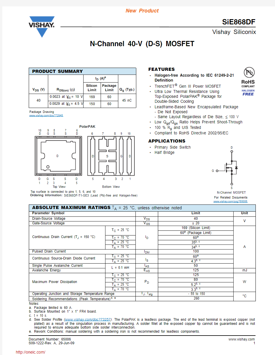
SiE868DF
Document Number: https://www.wendangku.net/doc/9518292691.html,
N-Channel 40-V (D-S) MOSFET
FEATURES
?Halogen-free According to IEC 61249-2-21
Definition
?TrenchFET ? Gen III Power MOSFET ?Ultra Low Thermal Resistance Using
Top-Exposed PolarPAK ? Package for Double-Sided Cooling
?Leadframe-Based New Encapsulated Package
- Die Not Exposed
- Same Layout Regardless of Die Size, ≤ 100 V ?Low Q gd /Q gs Ratio Helps Prevent Shoot-Through ?100 % R g and UIS Tested
?Compliant to RoHS Directive 2002/95/EC
APPLICATIONS
?Primary Side Switch ?Half Bridge
PRODUCT SUMMARY
V DS (V)R DS(on) (Ω)I D (A)a
Q g (Typ.)Silicon Limit Package
Limit 40
0.0023 at V GS = 10 V
1696045 nC
0.0029 at V GS = 4.5 V
150
60
Package Drawing
https://www.wendangku.net/doc/9518292691.html,/doc?72945
For Related Documents
https://www.wendangku.net/doc/9518292691.html,/ppg?65006
Notes:
a.Package limited is 60 A.
b.Surface Mounted on 1" x 1" FR4 board.
c.t = 10 s.
d.See Solder Profile (https://www.wendangku.net/doc/9518292691.html,/doc?73257). The PolarPAK is a leadless packag
e. The end of the lead terminal is exposed copper (not plated) as a result of the singulation process in manufacturing. A solder fillet at the exposed copper tip cannot be guaranteed and is not required to ensure adequate bottom side solder interconnection.
e.Rework Conditions: manual soldering with a soldering iron is not recommended for leadless components. ABSOLUTE MAXIMUM RATINGS T A = 25 °C, unless otherwise noted
Parameter Symbol Limit Unit
Drain-Source Voltage V DS 40
V
Gate-Source Voltage
V GS ± 20Continuous Drain Current (T J = 150 °C)T C = 25 °C
I D 169 (Silicon Limit)
A 60a (Package Limit)
T C = 70 °C 60a
T A = 25 °C 35b, c
T A = 70 °C 34b, c
Pulsed Drain Current I DM 100
Continuous Source-Drain Diode Current T C = 25 °C I S 60a
T A = 25 °C 4.3b, c
Single Pulse Avalanche Current L = 0.1 mH
I AS 50
Avalanche Energy
E AS 125mJ Maximum Power Dissipation
T C = 25 °C
P D 125W T C = 70 °C 80
T A = 25 °C 5.2b, c T A = 70 °C 3.3b, c
Operating Junction and Storage Temperature Range T J , T stg - 55 to 150
°C Soldering Recommendations (Peak Temperature)
d, e 260
https://www.wendangku.net/doc/9518292691.html, Document Number: 65006Vishay Siliconix
SiE868DF
Notes:
a.Surface Mounted on 1" x 1" FR4 board.
b.Maximum under Steady State conditions is 68 °C/W.
c.Measured at source pin (on the side of the package).
Notes:
a. Pulse test; pulse width ≤ 300 μs, duty cycle ≤ 2 %.
b. Guaranteed by design, not subject to production testing.
Stresses beyond those listed under “Absolute Maximum Ratings” may cause permanent damage to the device. These are stress ratings only, and functional operation of the device at these or any other conditions beyond those indicated in the operational sections of the specifications is not implied. Exposure to absolute maximum rating conditions for extended periods may affect device reliability.
THERMAL RESISTANCE RATINGS
Parameter Symbol Typical Maximum Unit
Maximum Junction-to-Ambient
a, b t ≤ 10 s R thJA 2024°C/W Maximum Junction-to-Case (Drain Top)
Steady State R thJC (Drain)0.81Maximum Junction-to-Case (Source)
a, c R thJC (Source) 2.2 2.7SPECIFICATIONS T J = 25 °C, unless otherwise noted
Parameter Symbol Test Conditions Min.Typ.Max.Unit
Static
Drain-Source Breakdown Voltage V DS V GS = 0 V , I D = 250 μA
40
V V DS Temperature Coefficient ΔV DS /T J I D = 250 μA
45mV/°C
V GS(th) T emperature Coefficient ΔV GS(th)/T J - 5.5Gate-Source Threshold Voltage V GS(th)V DS = V GS , I D = 250 μA 1.0 1.6
2.2V Gate-Source Leakage
I GSS
V DS = 0 V , V GS = ± 20 V ± 100nA Zero Gate Voltage Drain Current I DSS V DS = 40 V , V GS = 0 V
1μA V DS = 40 V, V GS = 0 V , T J = 55 °C
10On-State Drain Current a
I D(on) V DS ≥ 5 V , V GS = 10 V 25
A
Drain-Source On-State Resistance a R DS(on)V GS = 10 V, I D = 20 A 0.00180.0023ΩV GS = 4.5 V , I D = 20 A 0.00240.0029
Forward T ransconductance a g fs V DS = 15 V, I D = 20 A
105S
Dynamic b
Input Capacitance C iss V DS = 20 V , V GS = 0 V , f = 1 MHz 6100pF
Output Capacitance
C oss 700Reverse Transfer Capacitance C rss 320Total Gate Charge
Q g V DS = 20 V , V GS = 10 V , I D = 20 A 95145nC
V DS = 20 V , V GS = 4.5 V , I D = 20 A
4565
Gate-Source Charge Q gs 17Gate-Drain Charge Q gd 12Gate Resistance R g f = 1 MHz
0.2
1.1
2.2Ω
Turn-On Delay Time t d(on) V DD = 20 V, R L = 2 Ω
I D ? 10 A, V GEN = 4.5 V , R g = 1 Ω
4060ns
Rise Time
t r 165250Turn-Off Delay Time t d(off) 65100Fall Time
t f 110165Turn-On Delay Time t d(on) V DD = 20 V, R L = 2 Ω
I D ? 10 A, V GEN = 10 V , R g = 1 Ω
1525Rise Time
t r 1525Turn-Off Delay Time t d(off) 5075Fall Time
t f 10
15Drain-Source Body Diode Characteristics Continuous Source-Drain Diode Current
I S
T C = 25 °C
60A Pulse Diode Forward Current a
I SM 100Body Diode Voltage
V SD I S = 10 A 0.8 1.2V Body Diode Reverse Recovery Time
t rr I F = 10 A, dI/dt = 100 A/μs, T J = 25 °C
5075ns Body Diode Reverse Recovery Charge
Q rr 75115
nC Reverse Recovery Fall Time
t a 30ns
Reverse Recovery Rise Time
t b 20
Document Number: https://www.wendangku.net/doc/9518292691.html,
Output Characteristics
On-Resistance vs. Drain Current
Gate Charge
Transfer Characteristics
Capacitance
On-Resistance vs. Junction Temperature
Threshold Voltage Single Pulse Power, Junction-to-Ambient
https://www.wendangku.net/doc/9518292691.html, Document Number: 65006
Document Number: https://www.wendangku.net/doc/9518292691.html,
Vishay Siliconix
SiE868DF
TYPICAL CHARACTERISTICS 25 °C, unless otherwise noted
* The power dissipation P D is based on T J(max) = 150 °C, using junction-to-case thermal resistance, and is more useful in settling the upper dissipation limit for cases where additional heatsinking is used. It is used to determine the current rating, when this rating falls below the package limit.
SiE868DF
Vishay Siliconix
TYPICAL CHARACTERISTICS 25 °C, unless otherwise noted
Normalized Thermal Transient Impedance, Junction-to-Case (Drain Top)
Normalized Thermal Transient Impedance, Junction-to-Source
Vishay Siliconix maintains worldwide manufacturing capability. Products may be manufactured at one of several qualified locations. Reliability data for Silicon Technology and Package Reliability represent a composite of all qualified locations. For related documents such as package/tape drawings, part marking, and reliability data, see https://www.wendangku.net/doc/9518292691.html,/ppg?65006.
https://www.wendangku.net/doc/9518292691.html, Document Number: 65006
Package Information
Vishay Siliconix POLARPAK? OPTION L
Document Number: https://www.wendangku.net/doc/9518292691.html,
Package Information Vishay Siliconix
Notes
Millimeters govern over https://www.wendangku.net/doc/9518292691.html,LIMETERS INCHES
DIM MIN.NOM.MAX.MIN.NOM.MAX.
A0.750.800.850.0300.0310.033
A10.00-0.050.000-0.002
b10.480.580.680.0190.0230.027
b20.410.510.610.0160.0200.024
b3 2.19 2.29 2.390.0860.0900.094
b40.89 1.04 1.190.0350.0410.047
b50.230.330.430.0090.0130.017
c0.200.250.300.0080.0100.012
D 6.00 6.15 6.300.2360.2420.248
D1 5.74 5.89 6.040.2260.2320.238
E 5.01 5.16 5.310.1970.2030.209
E1 4.75 4.90 5.050.1870.1930.199
H10.23--0.009--
H20.45-0.560.018-0.022
H30.310.410.510.0120.0160.020
H40.45-0.560.018-0.022
K1 4.22 4.37 4.520.1660.1720.178
K2 1.08 1.13 1.180.0430.0440.046
K3 1.37--0.054--
K40.24--0.009--
M1 4.30 4.50 4.700.1690.1770.185
M2 3.43 3.58 3.730.1350.1410.147
M30.22--0.009--
M40.05--0.002--
P10.150.200.250.0060.0080.010
T1 3.48 3.64 4.100.1370.1430.161
T20.560.760.950.0220.0300.037
T3 1.20--0.047--
T4 3.90--0.153--
T500.180.360.0000.0070.014
θ0°10°12°0°10°12°ECN: T-08441-Rev. C, 11-Aug-08
DWG: 5946
https://www.wendangku.net/doc/9518292691.html, Document Number: 72945
Application Note 826
Vishay Siliconix
A P P L I C A T I O N N O T E
RECOMMENDED MINIMUM PADS FOR PolarPAK ? Option L and S
Return to Index
Legal Disclaimer Notice https://www.wendangku.net/doc/9518292691.html, Vishay
Disclaimer
ALL PRODU CT, PRODU CT SPECIFICATIONS AND DATA ARE SU BJECT TO CHANGE WITHOU T NOTICE TO IMPROVE RELIABILITY, FUNCTION OR DESIGN OR OTHERWISE.
Vishay Intertechnology, Inc., its affiliates, agents, and employees, and all persons acting on its or their behalf (collectively,“Vishay”), disclaim any and all liability for any errors, inaccuracies or incompleteness contained in any datasheet or in any other disclosure relating to any product.
Vishay makes no warranty, representation or guarantee regarding the suitability of the products for any particular purpose or the continuing production of any product. To the maximum extent permitted by applicable law, Vishay disclaims (i) any and all liability arising out of the application or use of any product, (ii) any and all liability, including without limitation special, consequential or incidental damages, and (iii) any and all implied warranties, including warranties of fitness for particular purpose, non-infringement and merchantability.
Statements regarding the suitability of products for certain types of applications are based on Vishay’s knowledge of typical requirements that are often placed on Vishay products in generic applications. Such statements are not binding statements about the suitability of products for a particular application. It is the customer’s responsibility to validate that a particular product with the properties described in the product specification is suitable for use in a particular application. Parameters provided in datasheets and/or specifications may vary in different applications and performance may vary over time. All operating parameters, including typical parameters, must be validated for each customer application by the customer’s technical experts. Product specifications do not expand or otherwise modify Vishay’s terms and conditions of purchase, including but not limited to the warranty expressed therein.
Except as expressly indicated in writing, Vishay products are not designed for use in medical, life-saving, or life-sustaining applications or for any other application in which the failure of the Vishay product could result in personal injury or death. Customers using or selling Vishay products not expressly indicated for use in such applications do so at their own risk and agree to fully indemnify and hold Vishay and its distributors harmless from and against any and all claims, liabilities, expenses and damages arising or resulting in connection with such use or sale, including attorneys fees, even if such claim alleges that Vishay or its distributor was negligent regarding the design or manufacture of the part. Please contact authorized Vishay personnel to obtain written terms and conditions regarding products designed for such applications.
No license, express or implied, by estoppel or otherwise, to any intellectual property rights is granted by this document or by any conduct of Vishay. Product names and markings noted herein may be trademarks of their respective owners.
Material Category Policy
Vishay Intertechnology, Inc. hereb y certifies that all its products that are identified as RoHS-Compliant fulfill the definitions and restrictions defined under Directive 2011/65/EU of The European Parliament and of the Council of June 8, 2011 on the restriction of the use of certain hazardous substances in electrical and electronic equipment (EEE) - recast, unless otherwise specified as non-compliant.
Please note that some Vishay documentation may still make reference to RoHS Directive 2002/95/EC. We confirm that all the products identified as being compliant to Directive 2002/95/EC conform to Directive 2011/65/EU.
Revision: 12-Mar-121Document Number: 91000
分销商库存信息: VISHAY
SIE868DF-T1-GE3