MSP430F2350IRHA中文资料
Less Than 1μs
D 16-Bit RISC Architecture,
62.5ns Instruction Cycle Time D Hardware Multiplier
D
Basic Clock Module Configurations:--Internal Frequencies up to 16MHz With Four Calibrated Frequencies to ±1%--Internal Very Low Power LF Oscillator --32-kHz Crystal --High-Frequency Crystal up to 16MHz --Resonator --External Digital Clock Source --External Resistor
D 16-Bit Timer_A With Three Capture/Compare Registers D 16-Bit Timer_B With Three Capture/Compare Registers
D
On-Chip Comparator for Analog Signal Compare Function or Slope A/D Conversion
D Brownout Detector
D
Serial Onboard Programming,
No External Programming Voltage Needed Programmable Code Protection by Security Fuse
D Bootstrap Loader in Flash Devices D On-Chip Emulation Module D
Family Members Include:MSP430F2330
8KB +256B Flash Memory 1KB RAM
MSP430F2350
16KB +256B Flash Memory 2KB RAM
MSP430F2370
32KB +256B Flash Memory 2KB RAM
D Available in 40-pin QFN Package
D
For Complete Module Descriptions,See the MSP430x2xx Family User’s Guide
description
The Texas Instruments MSP430family of ultralow-power microcontrollers consists of several devices featuring different sets of peripherals targeted for various applications.The architecture,combined with five low-power modes is optimized to achieve extended battery life in portable measurement applications.The devices feature a powerful 16-bit RISC CPU,16-bit registers,and constant generators that contribute to maximum code efficiency.The digitally controlled oscillator (DCO)allows wake-up from low-power modes to active mode in less than 1μs.
The MSP430F23x0series is an ultralow-power microcontroller with two built-in 16-bit timers,one universal serial communication interface (USCI),a versatile analog comparator,and 32I/O pins.
This integrated circuit can be damaged by ESD.Texas Instruments recommends that all integrated circuits be handled with appropriate precautions.Failure to observe proper handling and installation procedures can cause damage.ESD damage can range from subtle performance degradation to complete device failure.Precision integrated circuits may be more susceptible to damage because very small parametric changes could cause the device not to meet its published specifications.These devices have limited built-in ESD protection.
PRODUCTION DATA information is current as of publication date.Products conform to specifications per the terms of Texas Instruments standard warranty.Production processing does not necessarily include testing of all parameters.
Please be aware that an important notice concerning availability,standard warranty,and use in critical applications of Texas Instruments semiconductor products and disclaimers thereto appears at the end of this data sheet.
AVAILABLE OPTIONS
PACKAGED DEVICES T A PLASTIC40-PIN QFN
(RHA)
--40°C to85°C MSP430F2330IRHA MSP430F2350IRHA MSP430F2370IRHA
--40°C to105°C MSP430F2330TRHA MSP430F2350TRHA MSP430F2370TRHA
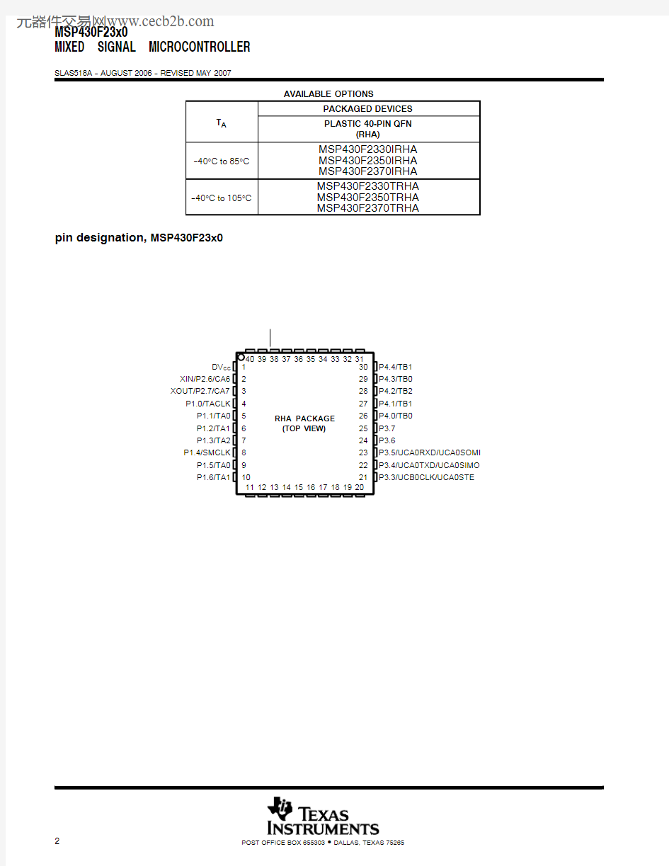
pin designation,MSP430F23x0
functional block diagram MSP430F23x0
Terminal Functions,MSP430F23x0
TERMINAL
NAME NO I/O
DESCRIPTION
DV CC1Digital supply voltage,positive terminal.Supplies all digital parts.
XIN/P2.6/CA62I/O Input terminal of crystal oscillator/general-purpose digital I/O pin/Comparator_A input
XOUT/P2.7/CA73I/O Output terminal of crystal oscillator/general-purpose digital I/O pin/Comparator_A input
P1.0/TACLK4I/O General-purpose digital I/O pin/Timer_A,clock signal TACLK input
P1.1/TA05I/O General-purpose digital I/O pin/Timer_A,capture:CCI0A input,compare:Out0output
P1.2/TA16I/O General-purpose digital I/O pin/Timer_A,capture:CCI1A input,compare:Out1output
P1.3/TA27I/O General-purpose digital I/O pin/Timer_A,capture:CCI2A input,compare:Out2output
P1.4/SMCLK8I/O General-purpose digital I/O pin/SMCLK signal output
P1.5/TA09I/O General-purpose digital I/O pin/Timer_A,compare:Out0output
P1.6/TA110I/O General-purpose digital I/O pin/Timer_A,compare:Out1output
P1.7/TA211I/O General-purpose digital I/O pin/Timer_A,compare:Out2output
P2.0/ACLK/CA212I/O General-purpose digital I/O pin/ACLK output/Comparator_A input
P2.1/TAINCLK/CA313I/O General-purpose digital I/O pin/Timer_A,clock signal at INCLK/Comparator_A input
P2.2/CAOUT/TA0/CA414I/O General-purpose digital I/O pin/Comparator_A output/Timer_A,capture:CCI0B input/Comparator_A
input
P2.3/CA0/TA115I/O General-purpose digital I/O pin/Comparator_A input/Timer_A,compare:Out1output
P2.4/CA1/TA216I/O General-purpose digital I/O pin/Comparator_A input/Timer_A,compare:Out2output
P2.5/R OSC/CA517I/O General-purpose digital I/O pin/input for external resistor defining the DCO nominal
frequency/Comparator_A input
P3.0/UCB0STE/
UCA0CLK
18I/O General-purpose digital I/O pin/USCIB0slave transmit enable/USCIA0clock input/output
P3.1/UCB0SIMO/
UCB0SDA
19I/O General-purpose digital I/O pin/USCIB0slave in/master out in SPI mode,SDA I2C data in I2C mode
P3.2/UCB0SOMI/
UCB0SCL
20I/O General-purpose digital I/O pin/USCIB0slave out/master in in SPI mode,SCL I2C clock in I2C mode
P3.3/UCB0CLK/
UCA0STE
21I/O General-purpose digital I/O/USCIB0clock input/output,USCIA0slave transmit enable
P3.4/UCA0TXD/ UCA0SIMO 22I/O General-purpose digital I/O pin/USCIA0transmit data output in UART mode,slave data in/master out in SPI mode
P3.5/UCA0RXD/ UCA0SOMI 23I/O General-purpose digital I/O pin/USCIA0receive data input in UART mode,slave data out/master in in SPI mode
P3.624I/O General-purpose digital I/O pin
P3.725I/O General-purpose digital I/O pin
P4.0/TB026I/O General-purpose digital I/O pin/Timer_B,capture:CCI0A input,compare:Out0output
P4.1/TB127I/O General-purpose digital I/O pin/Timer_B,capture:CCI1A input,compare:Out1output
P4.2/TB228I/O General-purpose digital I/O pin/Timer_B,capture:CCI2A input,compare:Out2output
P4.3/TB029I/O General-purpose digital I/O pin/Timer_B,capture:CCI0B input,compare:Out0output
P4.4/TB130I/O General-purpose digital I/O pin/Timer_B,capture:CCI1B input,compare:Out1output
P4.5/TB231I/O General-purpose digital I/O pin/Timer_B,compare:Out2output
P4.6/TBOUTH/ACLK32I/O General-purpose digital I/O pin/switch all PWM digital outputs to high impedance--Timer_B3:TB0to
TB2/ACLK output
P4.7/TBCLK33I/O General-purpose digital I/O pin/input clock TBCLK--Timer_B3
TDO/TDI34I/O Test data output port.TDO/TDI data output or programming data input terminal
TDI/TCLK35I Test data input or test clock input.The device protection fuse is connected to TDI/TCLK.
TMS36I Test mode select.TMS is used as an input port for device programming and test.
Terminal Functions(Continued)
TERMINAL
DESCRIPTION NAME NO I/O
TCK37I Test clock.TCK is the clock input port for device programming and test. RST/NMI38I Reset input,nonmaskable interrupt input port
D/AV SS39Digital/Analog supply voltage,negative terminal
AV CC40Analog supply voltage,positive terminal
QFN Pad NA NA QFN package pad connection to D/AV SS recommended
General-Purpose Register Program Counter Stack Pointer Status Register Constant Generator General-Purpose Register General-Purpose Register General-Purpose Register PC/R0SP/R1SR/CG1/R2CG2/R3R4R5R12R13General-Purpose Register General-Purpose Register R6R7General-Purpose Register General-Purpose Register R8R9General-Purpose Register General-Purpose Register R10R11General-Purpose Register General-Purpose Register
R14R15
short-form description
CPU
The MSP430CPU has a 16-bit RISC architecture that is highly transparent to the application.All operations,other than program-flow instructions,are performed as register operations in conjunc-tion with seven addressing modes for source operand and four addressing modes for destina-tion operand.
The CPU is integrated with 16registers that provide reduced instruction execution time.The register-to-register operation execution time is one cycle of the CPU clock.
Four of the registers,R0to R3,are dedicated as program counter,stack pointer,status register,and constant generator respectively.The remain-ing registers are general-purpose registers.Peripherals are connected to the CPU using data,address,and control buses,and can be handled with all instructions.instruction set
The instruction set consists of 51instructions with three formats and seven address modes.Each instruction can operate on word and byte data.Table 1shows examples of the three types of instruction formats;the address modes are listed in Table 2.
Table 1.Instruction Word Formats
Dual operands,source-destination e.g.ADD R4,R5R4+R5------>R5Single operands,destination only e.g.CALL R8
PC ---->(TOS),R8---->PC Relative jump,un/conditional
e.g.JNE
Jump-on-equal bit =0
Table 2.Address Mode Descriptions
ADDRESS MODE
S D SYNTAX EXAMPLE OPERATION Register F F MOV Rs,Rd MOV R10,R11R10
---->R11
Indexed
F F MOV X(Rn),Y(Rm)MOV 2(R5),6(R6)
M(2+R5)---->M(6+R6)Symbolic (PC relative)
F F MOV EDE,TONI M(EDE)---->M(TONI)Absolute F F MOV &MEM,&TCDAT M(MEM)---->M(TCDAT)Indirect F MOV @Rn,Y(Rm)MOV @R10,Tab(R6)M(R10)---->M(Tab+R6)
Indirect autoincrement F MOV @Rn+,Rm MOV @R10+,R11M(R10)---->R11R10+2---->R10Immediate
F
MOV #X,TONI
MOV #45,TONI #45
---->M(TONI)
NOTE :S =source
D =destination
operating modes
The MSP430has one active mode and five software selectable low-power modes of operation.An interrupt event can wake up the device from any of the five low-power modes,service the request and restore back to the low-power mode on return from the interrupt program.
The following six operating modes can be configured by software:
D Active mode(AM)
--All clocks are active
D Low-power mode0(LPM0)
--CPU is disabled
ACLK and SMCLK remain active,MCLK is disabled
D Low-power mode1(LPM1)
--CPU is disabled
ACLK and SMCLK remain active,MCLK is disabled
DCO’s dc-generator is disabled if DCO not used in active mode
D Low-power mode2(LPM2)
--CPU is disabled
MCLK and SMCLK are disabled
DCO’s dc-generator remains enabled
ACLK remains active
D Low-power mode3(LPM3)
--CPU is disabled
MCLK and SMCLK are disabled
DCO’s dc-generator is disabled
ACLK remains active
D Low-power mode4(LPM4)
--CPU is disabled
ACLK is disabled
MCLK and SMCLK are disabled
DCO’s dc-generator is disabled
Crystal oscillator is stopped
interrupt vector addresses
The interrupt vectors and the power-up starting address are located in the address range0xFFFF--0xFFC0.The vector contains the16-bit address of the appropriate interrupt-handler instruction sequence.
INTERRUPT SOURCE INTERRUPT FLAG SYSTEM INTERRUPT WORD ADDRESS PRIORITY
Power-up
External Reset
Watchdog
Flash key violation
PC out of range(see Note1)
PORIFG
RSTIFG
WDTIFG
KEYV
(see Note2)
Reset0xFFFE31,highest
NMI
Oscillator Fault
Flash memory access violation
NMIIFG
OFIFG
ACCVIFG
(see Notes2&6)
(non)-maskable
(non)-maskable
(non)-maskable
0xFFFC30
Timer_B3TBCCR0CCIFG(see Note3)maskable0xFFFA29
Timer_B3TBCCR1and TBCCR2,
CCIFGs,TBIFG
(see Notes2&3)
maskable0xFFF828
Comparator_A+CAIFG maskable0xFFF627 Watchdog timer WDTIFG maskable0xFFF426 Timer_A3TACCR0CCIFG(see Note3)maskable0xFFF225
Timer_A3
TACCR1CCIFG,
TACCR2CCIFG,
TAIFG(see Notes2&3)
maskable0xFFF024
USCI_A0/USCI_B0Receive USCI_B0I2C Status UCA0RXIFG,UCB0RXIFG
(see Note2and4)
maskable0xFFEE23
USCI_A0/USCI_B0Transmit USCI_B0I2C Receive/Transmit UCA0TXIFG,UCB0TXIFG
(see Note2and5)
maskable0xFFEC22
0xFFEA21
0xFFE820
I/O port P2(eight flags)P2IFG.0to P2IFG.7
(see Notes2&3)
maskable0xFFE619
I/O port P1(eight flags)P1IFG.0to P1IFG.7
(see Notes2&3)maskable0xFFE418
0xFFE217
0xFFE016
(see Note7)0xFFDE15
(see Note8)0xFFDC--0xFFC014--0,lowest NOTES: 1.A reset is executed if the CPU tries to fetch instructions from within the module register memory address range(0x0000--0x01FF).
2.Multiple source flags.
3.Interrupt flags are located in the module.
4.In SPI mode:UCB0RXIFG.In I2C mode:UCALIFG,UCNACKIFG,ICSTTIFG,UCSTPIFG.
5.In UART/SPI mode:UCB0TXIFG.In I2C mode:UCB0RXIFG,UCB0TXIFG.
6.Non-maskable:the individual interrupt-enable bit can disable an interrupt event,but the general-interrupt enable cannot.
Non-maskable:neither the individual nor the general interrupt-enable bit will disable an interrupt event.
7.This location is used as bootstrap loader security key(BSLSKEY).
A0xAA55at this location disables the BSL completely.
A zero(0h)disables the erasure of the flash if an invalid password is supplied.
8.The interrupt vectors at addresses0xFFDC to0xFFC0are not used in this device and can be used for regular program code if
necessary.
special function registers
Most interrupt and module-enable bits are collected in the lowest address space.Special-function register bits not allocated to a functional purpose are not physically present in the device.This arrangement provides simple software access.
interrupt enable1and2
Address76543210
00h ACCVIE NMIIE OFIE WDTIE
WDTIE Watchdog Timer interrupt enable.Inactive if watchdog mode is selected.Active if Watchdog Timer is configured in interval timer mode.
OFIE Oscillator fault enable
NMIIE(Non)maskable interrupt enable
ACCVIE Flash access violation interrupt enable
Address76543210
01h UCB0TXIE UCB0RXIE UCA0TXIE UCA0RXIE
UCA0RXIE USCI_A0receive-interrupt enable
UCA0TXIE USCI_A0transmit-interrupt enable
UCB0RXIE USCI_B0receive-interrupt enable
UCB0TXIE USCI_B0transmit-interrupt enable
interrupt flag register1and2
Address76543210
02h NMIIFG RSTIFG PORIFG OFIFG WDTIFG
rw--0rw--(0)rw--(1)rw--1rw--(0) WDTIFG Set on Watchdog Timer overflow(in watchdog mode)or security key violation.
Reset on V CC power-up or a reset condition at RST/NMI pin in reset mode.
OFIFG Flag set on oscillator fault
RSTIFG External reset interrupt flag.Set on a reset condition at RST/NMI pin in reset mode.Reset on V CC power up
PORIFG Power-on interrupt flag.Set on V CC power up.
NMIIFG Set via RST/NMI pin
Address76543210
03h UCB0TX
IFG UCB0RX
IFG
UCA0TX
IFG
UCA0RX
IFG
UCA0RXIFG USCI_A0receive-interrupt flag UCA0TXIFG USCI_A0transmit-interrupt flag UCB0RXIFG USCI_B0receive-interrupt flag UCB0TXIFG USCI_B0transmit-interrupt flag
Legend rw:
rw-0,1:Bit can be read and written.
Bit can be read and written.It is Reset or Set by PUC. Bit can be read and written.It is Reset or Set by POR.
rw-(0,1):
SFR bit is not present in device
memory organization
MSP430F2330MSP430F2350MSP430F2370
Memory
Main:interrupt vector Main:code memory
Size
Flash
Flash
8KB Flash
0xFFFF--0xFFC0
0xFFFF--0xE000
16KB Flash
0xFFFF--0xFFC0
0xFFFF--0xC000
32KB
0xFFFF--0xFFC0
0xFFFF--0x8000
Information memory Size
Flash
256Byte
0x10FF--0x1000
256Byte
0x10FF--0x1000
256Byte
0x10FF--0x1000
Boot memory Size
ROM
1KB
0x0FFF--0x0C00
1KB
0x0FFF--0x0C00
1KB
0x0FFF--0x0C00
RAM Size1KB Byte
0x5FF--0x0200
2KB Byte
0x9FF--0x0200
2KB
0x09FF--0x0200
Peripherals16-bit
8-bit
8-bit SFR 0x01FF--0x0100
0x00FF--0x0010
0x000F--0x0000
0x01FF--0x0100
0x00FF--0x0010
0x000F--0x0000
0x01FF--0x0100
0x00FF--0x0010
0x000F--0x0000
bootstrap loader(BSL)
The MSP430bootstrap loader(BSL)enables users to program the flash memory or RAM using a UART serial interface.Access to the MSP430memory via the BSL is protected by user-defined password.For complete description of the features of the BSL and its implementation,see the Application report Features of the MSP430 Bootstrap Loader,Literature Number SLAA089.
BSL Function RHA Package Pins
Data Transmit5--P1.1
Data Receive14--P2.2
flash memory
The flash memory can be programmed via the JTAG port,the bootstrap loader,or in-system by the CPU.The CPU can perform single-byte and single-word writes to the flash memory.Features of the flash memory include:
D Flash memory has n segments of main memory and four segments of information memory(A to D)of64
bytes each.Each segment in main memory is512bytes in size.
D Segments0to n may be erased in one step,or each segment may be individually erased.
D Segments A to D can be erased individually,or as a group with segments0--n.
Segments A to D are also called information memory.
D Segment A contains calibration data.After reset segment A is protected against programming or erasing.
It can be unlocked but care should be taken not to erase this segment if the calibration data is required.
peripherals
Peripherals are connected to the CPU through data,address,and control busses and can be handled using all instructions.For complete module descriptions,refer to the MSP430x2xx Family User’s Guide. oscillator and system clock
The clock system is supported by the basic clock module that includes support for a32768-Hz watch crystal oscillator,an internal very low power,low frequency oscillator,an internal digitally-controlled oscillator(DCO) and a high frequency crystal oscillator.The basic clock module is designed to meet the requirements of both low system cost and low-power consumption.The internal DCO provides a fast turn-on clock source and stabilizes in less than1μs.The basic clock module provides the following clock signals:
D Auxiliary clock(ACLK),sourced from a32768-Hz watch crystal,a high frequency crystal or the internal very
low power LF oscillator.
D Main clock(MCLK),the system clock used by the CPU.
D Sub-Main clock(SMCLK),the sub-system clock used by the peripheral modules.
The DCO settings to calibrate the DCO output frequency are stored in the information memory segment A.
DCO Calibration Data(provided from factory in flash info memory segment A)
DCO Frequency Calibration Register Size Address
1MHz CALBC1_1MHZ byte0x10FF
CALDCO_1MHZ byte0x10FE
8MHz CALBC1_8MHZ byte0x10FD
CALDCO_8MHZ byte0x10FC
12MHz CALBC1_12MHZ byte0x10FB
CALDCO_12MHZ byte0x10FA
16MHz CALBC1_16MHZ byte0x10F9
CALDCO_16MHZ byte0x10F8
brownout
The brownout circuit is implemented to provide the proper internal reset signal to the device during power on and power off.
digital I/O
There are48-bit I/O ports implemented—ports P1through P4:
D All individual I/O bits are independently programmable.
D Any combination of input,output,and interrupt conditions is possible.
D Edge-selectable interrupt input capability for all the eight bits of ports P1and P2.
D Read/write access to port-control registers is supported by all instructions.
D Each I/O has an individually programmable pull--up/pull--down resistor.
The MSP430F23x0devices provide32total port I/O pins available externally.Please see the device pinout for more information.
watchdog timer+
The primary function of the watchdog timer(WDT+)module is to perform a controlled system restart after a software problem occurs.If the selected time interval expires,a system reset is generated.If the watchdog function is not needed in an application,the module can be configured as an interval timer and can generate interrupts at selected time intervals.
hardware multiplier
The multiplication operation is supported by a dedicated peripheral module.The module performs 16×16,16×8,8×16,and 8×8bit operations.The module is capable of supporting signed and unsigned multiplication as well as signed and unsigned multiply and accumulate operations.The result of an operation can be accessed immediately after the operands have been loaded into the peripheral registers.No additional clock cycles are required.
comparator_A+
The primary function of the comparator_A+module is to support precision slope analog--to--digital conversions,battery--voltage supervision,and monitoring of external analog signals.
timer_A3
Timer_A3is a 16-bit timer/counter with three capture/compare registers.Timer_A3can support multiple capture/compares,PWM outputs,and interval timing.Timer_A3also has extensive interrupt capabilities.Interrupts may be generated from the counter on overflow conditions and from each of the capture/compare registers.
Timer_A3Signal Connections
Input Pin Number
Device Input Signal
Module Input Name
Module Block
Module Output Signal
Output Pin Number
RHA RHA
4-P1.0
TACLK TACLK ACLK ACLK SMCLK
SMCLK Timer
NA
13-P2.1TAINCLK INCLK 5-P1.1TA0CCI0A 5-P1.114-P2.2
TA0CCI0B 9--P1.5
V SS GND CCR0
TA0
V CC
V CC 6-P1.2
TA1CCI1A 6-P1.2CAOUT (internal)
CCI1B 10-P1.6V SS GND CCR1
TA1
15-P2.3
V CC
V CC 7-P1.3
TA2CCI2A 7-P1.3ACLK (internal)
CCI2B 11-P1.7V SS GND CCR2
TA2
16-P2.4
V CC
V CC
timer_B3
Timer_B3is a16-bit timer/counter with three capture/compare registers.Timer_B3can support multiple capture/compares,PWM outputs,and interval timing.Timer_B3also has extensive interrupt capabilities.
Interrupts may be generated from the counter on overflow conditions and from each of the capture/compare registers.
Timer_B3Signal Connections
Input Pin Number
Device
Input Signal
Module
Input Name
Module
Block
Module
Output Signal
Output
Pin Number
RHA RHA 33-P4.7TBCLK TBCLK
ACLK ACLK
SMCLK SMCLK
Timer NA
TBCLK INCLK
26-P4.0TB0CCI0A26-P4.0 29-P4.3TB0CCI0B29-P4.3 DV SS GND
CCR0TB0
DV CC V CC
27-P4.1TB1CCI1A27-P4.1 30-P4.4TB1CCI1B30-P4.4 DV SS GND
CCR1TB1
DV CC V CC
28-P4.2TB2CCI2A28-P4.2 ACLK(internal)CCI2B31-P4.5 DV SS GND
CCR2TB2
DV CC V CC
USCI
The universal serial communication interface(USCI)module is used for serial data communication.The USCI module supports synchronous communication protocols like SPI(3or4pin),I2C and asynchronous communication protocols like UART,enhanced UART with automatic baudrate detection(LIN),and IrDA.
USCI A0provides support for SPI(3or4pin),UART,enhanced UART and IrDA.
USCI B0provides support for SPI(3or4pin)and I2C.
peripheral file map
PERIPHERALS WITH WORD ACCESS
Timer_B3Capture/compare register
Capture/compare register
Capture/compare register
Timer_B register
Capture/compare control
Capture/compare control
Capture/compare control
Timer_B control
Timer_B interrupt vector TBCCR2
TBCCR1
TBCCR0
TBR
TBCCTL2
TBCCTL1
TBCCTL0
TBCTL
TBIV
0x0196
0x0194
0x0192
0x0190
0x0186
0x0184
0x0182
0x0180
0x011E
Timer_A3Capture/compare register
Capture/compare register
Capture/compare register
Timer_A register
Capture/compare control
Capture/compare control
Capture/compare control
Timer_A control
Timer_A interrupt vector TACCR2
TACCR1
TACCR0
TAR
TACCTL2
TACCTL1
TACCTL0
TACTL
TAIV
0x0176
0x0174
0x0172
0x0170
0x0166
0x0164
0x0162
0x0160
0x012E
Flash Memory Flash control3
Flash control2
Flash control1FCTL3
FCTL2
FCTL1
0x012C
0x012A
0x0128
Hardware Multiplier Sum extend
Result high word
Result low word
Second operand
Multiply signed+accumulate/operand1
Multiply+accumulate/operand1
Multiply signed/operand1
Multiply unsigned/operand1SUMEXT
RESHI
RESLO
OP2
MACS
MAC
MPYS
MPY
0x013E
0x013C
0x013A
0x0138
0x0136
0x0134
0x0132
0x0130
Watchdog Timer+Watchdog/timer control WDTCTL0x0120
PERIPHERALS WITH BYTE ACCESS
USCI_B0USCI_B0transmit buffer
USCI_B0receive buffer
USCI_B0status
USCI_B0bit rate control1
USCI_B0bit rate control0
USCI_B0control1
USCI_B0control0
USCI_B0I2C slave address
USCI_B0I2C own address UCB0TXBUF
UCB0RXBUF
UCB0STAT
UCB0BR1
UCB0BR0
UCB0CTL1
UCB0CTL0
UCB0SA
UCB0OA
0x06F
0x06E
0x06D
0x06B
0x06A
0x069
0x068
0x011A
0x0118
USCI_A0USCI_A0transmit buffer
USCI_A0receive buffer
USCI_A0status
USCI_A0modulation control
USCI_A0baud rate control1
USCI_A0baud rate control0
USCI_A0control1
USCI_A0control0
USCI_A0IrDA receive control
USCI_A0IrDA transmit control
USCI_A0auto baud rate control UCA0TXBUF
UCA0RXBUF
UCA0STAT
UCA0MCTL
UCA0BR1
UCA0BR0
UCA0CTL1
UCA0CTL0
UCA0IRRCTL
UCA0IRTCTL
UCA0ABCTL
0x0067
0x0066
0x0065
0x0064
0x0063
0x0062
0x0061
0x0060
0x005F
0x005E
0x005D
PERIPHERALS WITH BYTE ACCESS(continued)
Basic Clock System+Basic clock system control3
Basic clock system control2
Basic clock system control1
DCO clock frequency control BCSCTL3
BCSCTL2
BCSCTL1
DCOCTL
0x0053
0x0058
0x0057
0x0056
Port P4Port P4resistor enable
Port P4selection
Port P4direction
Port P4output
Port P4input P4REN
P4SEL
P4DIR
P4OUT
P4IN
0x0011
0x001F
0x001E
0x001D
0x001C
Port P3Port P3resistor enable
Port P3selection
Port P3direction
Port P3output
Port P3input P3REN
P3SEL
P3DIR
P3OUT
P3IN
0x0010
0x001B
0x001A
0x0019
0x0018
Port P2Port P2resistor enable
Port P2selection
Port P2interrupt enable
Port P2interrupt edge select
Port P2interrupt flag
Port P2direction
Port P2output
Port P2input P2REN
P2SEL
P2IE
P2IES
P2IFG
P2DIR
P2OUT
P2IN
0x002F
0x002E
0x002D
0x002C
0x002B
0x002A
0x0029
0x0028
Port P1Port P1resistor enable
Port P1selection
Port P1interrupt enable
Port P1interrupt edge select
Port P1interrupt flag
Port P1direction
Port P1output
Port P1input P1REN
P1SEL
P1IE
P1IES
P1IFG
P1DIR
P1OUT
P1IN
0x0027
0x0026
0x0025
0x0024
0x0023
0x0022
0x0021
0x0020
Special Function SFR interrupt flag2
SFR interrupt flag1
SFR interrupt enable2
SFR interrupt enable1IFG2
IFG1
IE2
IE1
0x0003
0x0002
0x0001
0x0000
absolute maximum ratings (see Note 1)
Voltage applied at V CC to V SS --0.3V to +4.1V ....................................................Voltage applied to any pin (see Note 2)--0.3V to V CC +0.3V ........................................Diode current at any device terminal .±2mA ......................................................Storage temperature (unprogrammed device,see Note 3)--55°C to 150°C ............................Storage temperature (programmed device,see Note 3)--40°C to 105°C
..............................NOTES: 1.Stresses beyond those listed under “absolute maximum ratings”may cause permanent damage to the device.These are stress
ratings only,and functional operation of the device at these or any other conditions beyond those indicated under “recommended operating conditions”is not implied.Exposure to absolute-maximum-rated conditions for extended periods may affect device reliability.
2.All voltages referenced to V SS .The JTAG fuse-blow voltage,V FB ,is allowed to exceed the absolute maximum rating.The voltage
is applied to the TDI/TCLK pin when blowing the JTAG fuse.
3.Higher temperature may be applied during board soldering process according to the current JEDEC J--STD--020specification with
peak reflow temperatures not higher than classified on the device label on the shipping boxes or reels.
recommended operating conditions
PARAMETER
MIN NOM
MAX UNITS Supply voltage during program execution,V CC
AV CC =DV CC =V CC (see Note 1) 1.8 3.6V Supply voltage during flash memory programming,V CC AV CC =DV CC =V CC (see Note 1) 2.2 3.6V Supply voltage,V SS
AV SS =DV SS =V SS 0.00.0V free air range I Version --4085°C Operating free-air temperature range,T A
T Version
--40105°C
V CC =1.8V,
Duty Cycle =50%±10%
dc 4.15Processor frequency f SYSYTEM (Maximum MCLK frequency)(see Notes 2,3and
Figure 1)
V CC =2.7V,
Duty Cycle =50%
±10%dc 12MHz V CC ≥3.3V,
Duty Cycle =50%
±10%
dc
16
NOTES: 1.It is recommended to power AV CC and DV CC from the same source.A maximum difference of 0.3V between AV CC and DV CC can
be tolerated during power-up and operation.
2.The MSP430CPU is clocked directly with MCLK.
Both the high and low phase of MCLK must not exceed the pulse width of the specified maximum frequency.
3.Modules might have a different maximum input clock specification.See the specification of the respective module in this datasheet.
4.151216Supply Voltage --V
S y s t e m F r e q u e n c y --M H z
Supply voltage range during flash memory programming
Supply voltage range during program execution
7.5NOTE :Minimum processor frequency is defined by system clock.Flash program or erase operations require a minimum V CC of 2.2V.
Figure 1.Operating Area
electrical characteristics over recommended ranges of supply voltage and operating free-air temperature(unless otherwise noted)
active mode supply current(into V CC)excluding external current(see Notes1and2)
PARAMETER TEST CONDITIONS T A VCC MIN TYP MAX UNIT
Active mode f DCO=f MCLK=f SMCLK=1MHz,
f ACLK=32,768Hz,
Program executes from flash,
BCSCTL1CALBC11MHZ
2.2V270370
I AM,1MHz
(AM)
current(1MHz)
=CALBC1_1MHZ,
DCOCTL=CALDCO_1MHZ,
CPUOFF=0,SCG0=0,SCG1=0,
OSCOFF=0
3V390550
μA Active mode
f DCO=f MCLK=f SMCLK=1MHz,
f ACLK=32,768Hz,
Program executes in RAM,
BCSCTL1CALBC11MHZ
2.2V226
I AM,1MHz
(AM)
current(1MHz)
=CALBC1_1MHZ,
DCOCTL=CALDCO_1MHZ,
CPUOFF=0,SCG0=0,SCG1=0,
OSCOFF=0
3V318
μA
f MCLK=f SMCLK=
4,096Hz,
--40..85_C 2.2V26 Active mode
f ACLK=32,768Hz/8=
f DCO=0Hz,
Program executes in
105_C 2.2V14
I AM,4kHz
(AM)
current(4kHz)
flash,
SELMx=11,SELS=1,
DIVMx===--40..85_C3V39
μA DIVSx DIVAx11,
CPUOFF=0,SCG0=1,SCG1=0,
OSCOFF=0105_C3V17
f MCLK=f SMCLK=f DCO(0,0)≈100kHz,
0Hz
--40..85_C 2.2V6085 Active mode
f ACLK=0Hz,
Program105_C 2.2V95
I AM,100kHz
(AM)
current(100kHz)
executes in flash,
RSELx=0,DCOx=0,
0=00
--40..85_C3V7295
μA CPUOFF=0,SCG00,SCG1=0,
OSCOFF=1105_C3V105
NOTES: 1.All inputs are tied to0V or V CC.Outputs do not source or sink any current.
2.The currents are characterized with a Micro Crystal CC4V--T1A SMD crystal with a load capacitance of9pF.
The internal and external load capacitance is chosen to closely match the required9pF.
typical characteristics --active mode supply current (into DV CC +AV CC )
0.01.02.03.04.05.06.0
7.08.0
V CC --Supply Voltage --V A c t i v e M o d e C u r r e n t --m A
Figure 2.Active mode current vs V CC ,T A =25°C
0.01.0
2.0
3.0
4.05.0
f DCO --DCO Frequency --MHz
A c t i v e M o d e C u r r e n t --m A
Figure 3.Active mode current vs DCO frequency
electrical characteristics over recommended ranges of supply voltage and operating free-air temperature (unless otherwise noted)
low power mode supply currents (into V CC )excluding external current (see Notes 1and 2)
PARAMETER
TEST CONDITIONS
VCC MIN
TYP MAX UNIT f MCLK =0MHz,
1MHz T A =--40..85_C 2268
84μA Low-power mode
current f SMCLK =f DCO =1MHz,f ACLK =32,768Hz,
BCSCTL1CALBC11MHZ T A =105_C 2.2
V 90
μA I LPM0,1MHz
0(LPM0)current,see Note 3
=CALBC1_1MHZ,DCOCTL =CALDCO_1MHZ,100T A =--40..85_C 88
110μA _CPUOFF =1,SCG0=0,SCG1=0,OSCOFF =0
T A =105_C 3V
115
μA f MCLK =0MHz,
100kHz T A =--40..85_C 2236
45μA Low-power mode current f SMCLK =f DCO(0,0)≈100kHz,T A =105_C 2.2
V 50
μA I LPM0,100kHz
0(LPM0)current,Note 3
f ACLK =0Hz,
RSELx =0,DCOx =0,1=00T A =--40..85_C 40
50μA see CPUOFF =1,SCG00,SCG1=0,OSCOFF =1
T A =105_C 3V
54
μA f MCLK =f SMCLK =0MHz,f DCO =1MHz,32768Hz
T A =--40..85_C 2220
28μA Low-power mode
current f ACLK =32,768Hz,BCSCTL1=CALBC1_1MHZ,T A =105_C 2.2
V 32
μA I LPM2
2(LPM2)current,Note 4
DCOCTL =CALDCO_1MHZ,1=01T A =--40..85_C 23
32μA see CPUOFF =1,SCG00,SCG1=1,OSCOFF =0
T A =105_C 3V
37
μA
T A =--40..25°C
0.7
1.0f 0MHz T A =85°C
2.2V
3.3A Low-power mode current DCO =f MCLK =f SMCLK =0MHz,T A =105°C 10μI LPM3,LFXT1
3(LPM3)current,f ACLK =32,768Hz,
CPUOFF =1,SCG0=1,SCG1=1,0
T A =--40..25°C 0.85
1.2see Note 4
OSCOFF =T A =85°C 3V
3.8A T A =105°C 12μT A =--40..25°C
0.25
0.8f 0MHz
T A =85°C 2.2V
2.9A Low-power mode current (LPM3)DCO =f MCLK =f SMCLK =0MHz,T A =105°C 9μI LPM3,VLO
3current,f ACLK from internal LF oscillator (VLO),CPUOFF =1,SCG0=1,SCG1=1,0
T A =--40..25°C 0.35
1.0see Note 4
OSCOFF =T A =85°C 3V
3.5A T A =105°C 11μT A =--40°C 0.5T A =25°C
22V 0.5f 0MHz T A =85°C 2.2V
1.7
2.7μA Low-power mode current DCO =f MCLK =f SMCLK =0MHz,T A =105°C 8.6I LPM4
4(LPM4)current,Note 5
f ACLK =0Hz,
CPUOFF =1,SCG0=1,SCG1=1,1
T A =--40°C 0.5see OSCOFF =T A =25°C 0.5T A =85°C 3V
1.9
3μA T A =105°C
9
NOTES: 1.All inputs are tied to 0V or V CC .Outputs do not source or sink any current.
2.The currents are characterized with a Micro Crystal CC4V--T1A SMD crystal with a load capacitance of 9pF.
The internal and external load capacitance is chosen to closely match the required 9pF.3.Current for brownout and WDT clocked by SMCLK included.4.Current for brownout and WDT clocked by ACLK included.5.Current for brownout included.