A reconfigurable design-for-debug infrastructure of SoCs

A Reconfigurable Design-for-Debug
Infrastructure for SoCs
Miron Abramovici, Paul Bradley, Kumar Dwarakanath, Peter Levin, Gerard Memmi, Dave Miller
DAFCA, Inc.
10 Speen Street, Second Floor,
Framingham, MA 01701
+1 774 204 0020
{miron, paul, kumar, peter, gerard, davem}@https://www.wendangku.net/doc/af3408938.html,
ABSTRACT
In this paper we present a Design-for-Debug (DFD) reconfigurable infrastructure for SoCs to support at-speed in-system functional debug. A distributed reconfigurable fabric inserted at RTL provides a debug platform that can be configured and operated post-silicon via the JTAG port. The platform can be repeatedly reused to configure many debug structures such as assertions checkers, transaction identifiers, triggers, and event counters.
Categories and Subject Descriptors
B.7 [Integrated circuits]; J.6 [Computer-aided engineering] General Terms
Verification, Performance, Design, Economics, Experimentation. Keywords: Silicon debug, at-speed debug, assertion-based debug, what-if experiments.
1.THE PAIN OF SILICON DEBUG
Although the pre-silicon verification of new SoCs has made great progress, perfectly working first silicon is still the exception rather than the rule. In spite of huge efforts in design verification, errors are still found in about two thirds of newly manufactured SoCs. In most cases, the silicon validation process trying to answer the question “Does my system work correctly?” quickly becomes silicon debug trying to answer the question “Why doesn’t my system work?” First silicon debug requires a labor-intensive engineering effort of many months and, and as shown in Figure 1 [3], it has become the most time-consuming part – 35% on average - of the development cycle of a new chip. This confirms the ITRS roadmap statement that the time to locate the root cause of a problem grows exponentially with the advances in process technology that produce larger, denser, and more complex designs. Today most devices have short market windows, and the delays caused by inefficient and unpredictable debug significantly increase the time-to-market and result in a significant loss of market share, or even a complete loss of revenue.
Despite its growing importance, silicon debug currently lacks a standard methodology and a standard DFD infrastructure; also, very few commercially-available EDA tools address this problem. The most common existing tools are debuggers for embedded software [1] [8], but these tools provide only limited observability into the SoC hardware domain, mostly by monitoring processor busses. The most difficult part of the debug process is in-system at-speed debug where, unlike in a tester-based debug environment, we do not have access to the I/O pins of the SoC under debug, and, in general, expected values are not known. However, in-system (in-situ) validation is always required, since it typically provides the most comprehensive functional exercise of the new chip in its target environment. Note than even when a new SoC is “perfect”, its lack of internal observability still makes its in-system validation a long and difficult process.
There is a huge difference between the variety and the sophistication of the tools available for pre-silicon verification and the lack of automation associated with post-silicon validation. Access methods based on physical effects (thermal emissions, radiation, etc.) may provide good observability, but they are very slow and rely on expensive hardware and/or cumbersome procedures. Most in-house techniques rely on ad-hoc DFD structures added to the design to provide some internal observability. However, the DFD logic is design-specific, there are no automatic tools to insert it or to process the information it provides, and in general, there is little reuse from project to project. The software necessary to configure and operate custom
Permission to make digital or hard copies of all or part of this work for personal or classroom use is granted without fee provided that copies are not made or distributed for profit or commercial advantage and that copies bear this notice and the full citation on the first page. To copy otherwise, or republish, to post on servers or to redistribute to lists, requires prior specific permission and/or a fee.
DAC 2006, July 24–28, 2006, San Francisco, California, USA. Copyright 2006 ACM 1-59593-381-6/06/0007…$5.00.
130nm
Spec RTL Netlist Si Debug
> 28%
>35%?
~ 17%
Figure 1:Silicon debug vs. time-to-market
2.2
instrumentation is often inadequate. Manual instrumentation of thousands of signals takes a long time, is error-prone, and cannot easily accommodate subsequent design changes. Ad-hoc methods do not scale well for future designs.
A comprehensive review of prior work on DFD techniques can be found in [10]. Most of prior work deals with in-house solutions for different custom microprocessors.
2. A NEW APPROACH TO DFD
By definition, any hardware debug process has to deal with unpredictable problems, so ideally we would like to be able to create the DFD structures needed to investigate issues only after we know where they are and their nature. Dynamically creating new hardware structures in existing silicon is a feature of reconfigurable logic. The conventional form of reconfigurable logic that can be used in an SoC is an embedded FPGA, but once the FPGA core has been placed in a certain spot in the SoC, observing and controlling many different signals from different areas of the SoC, is likely to make the SoC unroutable. In contrast, our approach relies on a new form of reconfigurable logic, namely a distributed reconfigurable fabric, whose components are inexpensive DFD instruments that can be widely distributed and can observe thousands of signals.
The instruments are generated on-the-fly for the target SoC based on user guidance. The models of generated instruments are automatically inserted in the RTL model of the SoC and the instrumented RTL design goes through the normal synthesis and physical design flow. Thus the instrumentation process is compatible with the existing design flows. The idea of inserting reconfigurable logic at RTL was previously used in [9].
2.1 DFD Instruments
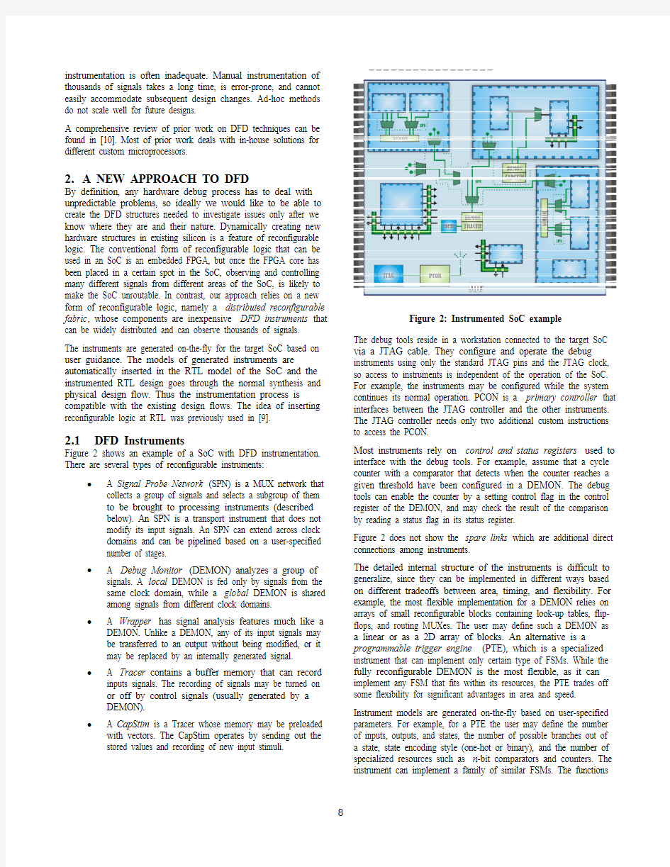
Figure 2 shows an example of a SoC with DFD instrumentation. There are several types of reconfigurable instruments:
? A Signal Probe Network (SPN) is a MUX network that collects a group of signals and selects a subgroup of them
to be brought to processing instruments (described
below). An SPN is a transport instrument that does not
modify its input signals. An SPN can extend across clock
domains and can be pipelined based on a user-specified
number of stages.
? A Debug Monitor (DEMON) analyzes a group of signals. A local DEMON is fed only by signals from the
same clock domain, while a global DEMON is shared
among signals from different clock domains.
? A Wrapper has signal analysis features much like a DEMON. Unlike a DEMON, any of its input signals may
be transferred to an output without being modified, or it
may be replaced by an internally generated signal.
? A Tracer contains a buffer memory that can record inputs signals. The recording of signals may be turned on
or off by control signals (usually generated by a
DEMON).
? A CapStim is a Tracer whose memory may be preloaded with vectors. The CapStim operates by sending out the
stored values and recording of new input stimuli. The debug tools reside in a workstation connected to the target SoC via a JTAG cable. They configure and operate the debug instruments using only the standard JTAG pins and the JTAG clock, so access to instruments is independent of the operation of the SoC. For example, the instruments may be configured while the system continues its normal operation. PCON is a primary controller that interfaces between the JTAG controller and the other instruments. The JTAG controller needs only two additional custom instructions to access the PCON.
Most instruments rely on control and status registers used to interface with the debug tools. For example, assume that a cycle counter with a comparator that detects when the counter reaches a given threshold have been configured in a DEMON. The debug tools can enable the counter by a setting control flag in the control register of the DEMON, and may check the result of the comparison by reading a status flag in its status register.
Figure 2 does not show the spare links which are additional direct connections among instruments.
The detailed internal structure of the instruments is difficult to generalize, since they can be implemented in different ways based on different tradeoffs between area, timing, and flexibility. For example, the most flexible implementation for a DEMON relies on arrays of small reconfigurable blocks containing look-up tables, flip-flops, and routing MUXes. The user may define such a DEMON as a linear or as a 2D array of blocks. An alternative is a programmable trigger engine (PTE), which is a specialized instrument that can implement only certain type of FSMs. While the fully reconfigurable DEMON is the most flexible, as it can implement any FSM that fits within its resources, the PTE trades off some flexibility for significant advantages in area and speed. Instrument models are generated on-the-fly based on user-specified parameters. For example, for a PTE the user may define the number of inputs, outputs, and states, the number of possible branches out of a state, state encoding style (one-hot or binary), and the number of specialized resources such as n-bit comparators and counters. The instrument can implement a family of similar FSMs. The functions Figure 2: Instrumented SoC example
that determine the detailed operation of a particular FSM are configured at run-time.
2.2Debug Paradigms
The reconfigurable debug platform supports several debug paradigms, namely signal capture, assertion-based debug, event-driven analysis, stimulate-and-capture, and what-if experiments. These paradigms can be easily intermixed. Each paradigm requires interactions among several debug instruments.
The basic paradigm is signal capture. The user configures SPNs to select the group of signals to be concurrently recorded in a trace buffer. The SPN delivers the selected group to both a Tracer and a DEMON. The DEMON outputs are connected to Tracer inputs. The DEMON is configured to implement triggers (event detectors), which are used to start or stop recording by the Tracer. A Tracer may be programmed to stop recording once its buffer fills up, or to continuously record in a circular buffer until triggered to stop. The full flag of the trace buffer is available as a status flag that can be checked by the debug tools. When recording stops, the contents of the buffer can be downloaded into the workstation and converted into a VCD or FSDB file that is processed by a waveform display tool such as VERDI [5]. Thus the user can view the signals coming from silicon exactly the same way as signals coming from simulation. Unlike in simulation, where the user can examine any signal, in silicon only a subset of signals can be recorded. A post-processing algorithm [6] can infer the expected values of some of the uninstrumented signals.
Assertion-based debug is a well-known paradigm very successfully used in pre-silicon verification. While the analysis of the captured waveforms to detect misbehavior is an intensive manual effort, assertions perform automatic checks of relationships among signals. Without assertions, an internal error may take thousands of cycles to reach an observable output, which makes backtracing from the observed error to its root cause a difficult process. In contrast, when an assertion fires, we are much closer to the source of the problem, both in time and in the circuit space; thus error detection by firing assertions provides a significant reduction in the search space. Thus assertions are important because they improve the observability of internal errors. The reconfigurable debug platform brings the benefits of assertions to in-system at-speed silicon debug of SoCs. The debug tools can dynamically configure assertions in DEMONs. Since most assertions check relations between signals and do not rely on expected values, they provide a perfect match for the system debug environment where expected values are usually not known. Assertions implemented in a local DEMON are driven by the same functional clock of the clock domain where the inputs analyzed by the assertion reside. An assertion implemented in a global DEMON works at a clock frequency higher than or equal to the frequency of the fastest clock domain providing inputs to the DEMON. All the enabled assertions can work concurrently.
Because assertions are dynamically created in reconfigurable logic, many different assertions may be configured in the same infrastructure logic at different times during operation. While hundreds of assertions can be used in simulation, the number of assertions that can be configured concurrently in the fabric is limited by the fabric capacity and by the resources required to implement each assertion. However, we can take advantage of the reusability of the reconfigurable logic by partitioning the set of desired assertions into groups, and downloading one group at a time. In a system processing a non-repetitive continuous stream of data (such as music or video), this process can be automated so that each group runs in turn for a predetermined time period. Such an assertion loop provides a powerful silicon debug mechanism.
We can use an assertion firing as a trigger to stop recording of signals in the Tracer. In this way the contents of the trace buffer represents the most recent activity preceding the assertion firing and it is likely to provide good clues about the misbehavior that made the assertion fail. Note that a few clock cycles may elapse between the firing of the assertion fires and the time when recording stops. This known latency should be taken into account when analyzing the events stored in the trace buffer.
Event-driven analysis recognizes specific events occurring in the SoC and uses these events to initiate appropriate debug activities. For example, consider an assertion checking a relation that is supposed to be valid only after a certain event has occurred. Then we configure the trigger that detects the event, and we use the output of this trigger to enable the assertion checker. Note that the trigger and the assertion checker may reside in the same or in different DEMONs. If the two separate DEMONs are both local the trigger output should be routed on a spare link between the two instruments. If the trigger resides in a local DEMON and the assertion is configured in a global DEMON, the trigger output can also be routed via the SPN to reach the assertion.
A transaction is a sequence of related events occurring in the SoC – for example, a request→acknowledge→grant sequence, a DMA transfer, sending of a packet, etc. Transaction-level modeling has been proven to be very beneficial in pre-silicon verification, since it raises the level of abstraction used in debugging. The events of a transaction often follow a cause-effect chain, which can be easily traced going forwards or backwards in time. It is often more effective to follow a sequence of transactions than to analyze their corresponding bit-level waveforms.
A difficult problem for in-system debug is the apparent non-determinism in error occurrence. Because of many asynchronous activities taking place in a system, the same error may occur at different clock cycles in repeated experiments. Transactions can also help creating reproducible errors, as many errors that are not reproducible in terms of absolute clock cycle counts are reproducible in terms of a sequence of transactions.
The same trigger circuit that identifies a transaction can also be used as an assertion checker. For example, consider a transaction T consisting of a first event Event1 followed by 5 occurrences of the Event2, where the last Event2 is supposed to arrive in at most 10 clock cycles after the first one. (Assume that Event1 and Event2 are mutually exclusive.) To recognize T, we need an FSM that includes triggers for Event1 and Event2, a cycle counter, and an Event2 counter. The circuit whose output identifies T can be easily modified to implement an assertion checking that after Event1, the 5th Event2 does arrive within the specified interval (Figure 3).
In the stimulate-and-capture paradigm, we use a CapStim instrument whose buffer contains stimuli to be applied to another functional block. The connections between CapStim and the target block have been specified at the instrumentation time. For example, if the inputs of the target block are supplied by a bus, we can enable CapStim to drive the same bus, while outputs from the target block can be connected via an SPN to inputs of CapStim. The source for the stimuli stored in the buffer could be external to SoC (then the vectors are uploaded via JTAG), or they could be captured during the preceding operation of the chip. One possible scenario is to monitor signals from the target block and have a trigger to detect reaching of a specific state. We use the trigger signal to enable CapStim to take control of the bus, and then to apply the stored vectors as stimuli for the target block. While the vectors are applied, output signals from the target block may be recorded by CapStim replacing the already applied vector. Many other scenarios are possible.
What-if experimentation is a paradigm that allows the user to override system signals with signals generated in Wrappers. Any wrapped user signal can traverse the Wrapper “as is” or it can be replaced by a signal generated in the Wrapper. For example, assume that at some point in the debug process, the user has two suspect sources that converge in an area where an error has been detected, but it is difficult to determine which suspect is the real culprit. If a control signal that selects the source has been wrapped, then the user may force a constant value on this signal so that one of the sources is selected. This experiment, followed by a similar one that forces the other source to be selected, is sufficient to solve this problem.
Many systems used in high-reliability applications are required to tolerate errors or defects that occur during operation. The evaluation
process of these features is usually based on fault simulation, which is computationally very expensive, as it typically deals with one fault at-a-time, and the entire system needs to be simulated. The reconfigurable fabric can be used in another what-if experiment to provide a very efficient fault injection mechanism. An experiment consists in injecting a fault on a wrapped signal, and observing the resulting system behavior, which may be checked with assertions. Such an experiment proceeds at the real operation speed and a large number of fault types (single or multiple stuck faults, opens, shorts, delay faults, intermittent faults, functional faults, single event upsets, and so on) can be easily created and injected.
3. WHAT SIGNALS TO INSTRUMENT?
Most debug paradigms rely on tapping user signals and connecting the tapped signals to debug instruments. To be able to determine where errors are coming from, we would like to examine signals that originate in areas more likely to have errors. Hence the first question is to determine the high-risk areas in the design. The typical high-risk areas are new user logic, new IP cores, and logic that was not fully verified pre-silicon.
Logic blocks that passed formal verification can be considered fully verified, except for potential timing problems. The completeness of verification is estimated by different measures such as code coverage or assertion coverage. New IP cores or new user logic may have areas with different degrees of coverage, and the focus should be on those blocks with less coverage.
Note that even a fully verified block, or a fully verified assertion, may still fail in silicon because of process variations. Because there are no guarantees that errors will never originate in a certain area, the risk estimates have a probabilistic nature. So the fully verified logic is less likely to have errors than logic with lower verification coverage.
In general, logic errors are much more likely to appear in control logic of interconnected FSMs than in the data paths. Hence, FSM signals from high-risk areas are the primary candidates for tapping. In addition, signals identifying important transactions are also good candidates to tap, since they provide high-level information very useful in understanding what is going on in the SoC; these signals are not limited to high-risk areas. If the user logic does not identify the desired transactions, the necessary logic can be configured in DEMONs; this requires tapping the signals needed by the triggers that recognize transactions.
If the user plans to implement specific assertions in silicon, the inputs to be checked by these assertions should be also tapped. Signals likely to be overridden in what-if experiments should be wrapped. Note that a signal to be wrapped should not be brought to its Wrapper via a MUX selection, because all wrapped signals (that are not overridden) should be able to go unmodified through the Wrapper.
Unlike tapping a signal that adds only an additional load to a user signal, wrapping a signal has more impact on timing, because it adds a replacement MUX in the path of the wrapped signal. At the same time, wrapping signals requires more area since every wrapped signal requires two Wrapper pins and a half of a Wrapper block.
Figure 3: Example for combined trigger and assertion
The user may allocate a budget for the area allocated for DFD instrumentation, and list the signals to tap or wrap in their priority order. Then the DFD instrumentation can be progressively added until the entire budget is used. As an example, in a chip with about 5M gates, an area increase of about 4% allows thousands of signals can be observed by a global DEMON and a 2K-deep trace buffer. Wrapping several hundreds of signals for what-if experiments requires a similar investment.
4.CREATING PERSONALITIES
The most basic means to create the needed debug structures in the reconfigurable fabric is the Personality Editor – a GUI that allows low-level direct access to functions of the look-up tables and routing structures.
The user can also access libraries of common hardware structures such as counters, comparators, decoders. They can be used directly or can be modified using the Personality Editor. A library of configurations for OVL assertions [11] is also available. Using an analogy with programming languages, the Personality Editor is equivalent to an assembly language, while the libraries are similar to macros.
FSMs can be described in a simple language for state tables. The compiler for state table descriptions generates the corresponding configuration bitstreams.
Verilog models provide the most flexible means of modeling hardware for the debug instruments. Both the state table compiler and the Verilog compiler rely on a common set of algorithms for mapping the logic into look-up tables, for placing these in DEMON cells, establishing the connections among the cells, and translating the results into configuration bitstreams.
5.OTHER APPLICATIONS
The reconfigurable fabric provides a reconfigurable infrastructure platform that can be used in many other applications in addition to debug; some of these applications are briefly described below. Performance measurements rely on identifying and counting transactions; other triggers can be used to start and stop a measurement. For example, one can devise a circuit to determine the latency of a bus transfer, or to count cache hits and cache misses for a certain interval. Other simple performance measurements could be the utilization of a FIFO buffer (percentage of time when it is empty) or statistics of its high-water marks (how much of its capacity is used). Unlike software implementations of performance measurements that usually modify the data they attempt to measure, measurements implemented in hardware are non-intrusive.
On-line testing is a requirement for mission-critical applications, such as automotive, defense, aerospace, and medical electronics, where SoCs may be deployed for many years in harsh, hostile, remote, and/or difficult-to-access environments, and where the cost of in-field failures is extremely high. We can configure assertions in the fabric and let them run during normal operation to check important properties of a safe behavior. It is possible to implement more monitoring functions than the capacity of the fabric allows, by partitioning the functions into several groups and configuring and running one group at a time.
Soft error-fixing is another potential use of the reconfigurable infrastructure fabric. For this application, at least one wrapped signal is replaced by a signal computed in the Wrapper. The corrected signal may be the output of simple combinational function such an inverter to account for incorrect or misunderstood core specifications; more complex functions are possible if they can be implemented in the Wrapper. Note that the system with the fix logic may not be able to work at the target speed, but if the clock frequency can be adjusted for debug, such a fix can enable the debug work to continue without a respin, or can allow early samples to be sent to a customer.
6.AN EXPERIMENTAL CHIP
Figure 4 shows the layout of the first experimental SoC featuring a reconfigurable debug platform. The chip includes a LEON processor and a cryptography core, and it was designed at the University of Tennessee [4]. The chip is currently being manufactured by MOSIS.
.
Another experimental chip project using the reconfigurable debug instruments is described in [2]. Several industrial SoC designs using this technology are underway and will tapeout in the near future. 7.CONCLUSIONS
We have introduced a novel DFD methodology, based on a distributed reconfigurable fabric inserted in the RTL model of a design. The fabric provides a reconfigurable infrastructure platform that can implement many debug structures and can support many debug paradigms as well as many other applications. This technology brings unprecedented debug capabilities to in-system at-speed silicon debug of complex SoCs.
8.ACKNOWLEDGMENTS
This work has been supported in part by the NIST Advanced Technology Program, award number 70NANB4H3049.
We also acknowledge the tremendous work of our DAFCA colleagues.
9.REFERENCES
[1] A. Berent. Debugging Techniques for Embedded Systems
using Real-Time Software Trace.
https://www.wendangku.net/doc/af3408938.html,/pdfs/CoresightWhitepaper.pdf
Figure 4: Layout of experimental chip
[2]J. Bower, O. Mencer, W. Luck, and M. Abramovici. An SoC
with Reconfigurable Debug Infrastructure. Proceedings of
COOL Chips IX Conf., April 2006
[3]Collett ASIC/IC Verification Study, 2004 (data for 180nm and
130nm)
[4]Jiang, W., T. Marwah and D. Bouldin. Enhancing Reliability
and Flexibility of a System-on-Chip Using Reconfigurable
Logic. Proc. of the Midwest Symp. on Circuits and Systems,
Aug. 2005.
[5]Y. Hsu, B. Tabbara, Y. Chen, and F. Tsai. Advanced
Techniques for RTL Debugging. Proc 40th Design Automation Conf., June, 2003.
[6]Y.Hsu. Visibility Enhancement for Silicon Debug. Proc. 43rd
Design Automation Conf., July, 2006. [7]N. Kafafi, K. Bozman, and S.J.E. Wilton. Architectures and
Algorithms for Synthesizable Embedded Programmable Logic Cores. Proc. ACM/SIGDA Intn’l. Symp. on FPGAs, Febr. 2003 [8]R. Leatherman, B. Ableidinger, and N. Stollon. Processor and
System Bus On-Chip Instrumentation. Proc. Embedded
Systems Conference, April 2003.
[9]N. Kafafi, K. Bozman, and S.J.E. Wilton. Architectures and
Algorithms for Synthesizable Embedded Programmable Logic Cores. Proc. ACM/SIGDA Intn’l. Symp. on FPGAs, Febr. 2003 [10]B. Vermeulen and S.K. Goel. Design for Debug: Catching
Design Errors in Digital Chips. IEEE Design & Test of
Computers, May/June 2002
[11]https://www.wendangku.net/doc/af3408938.html,/activities/ovl/