LMV321IDBVR,LMV321IDBVR,LMV321IDBVR,LMV358IPWR,LMV324IPWR,LMV324IPWR, 规格书,Datasheet 资料
1
2
3
4
5
6
7
14
13
12
11
10
9
8
1OUT
1IN–
1IN+
V CC+
2IN+
2IN–
2OUT
4OUT
4IN–
4IN+
GND
3IN+
3IN–
3OUT
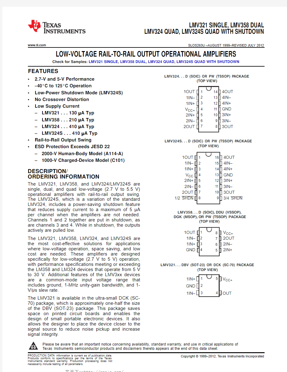
LMV324...D (SOIC) OR PW (TSSOP) P ACKAGE
(TOP VIEW)
LMV358...D (SOIC),DDU (VSSOP),
DGK (MSOP),OR PW (TSSOP) PACKAGE
(TOP VIEW)
1
2
3
4
8
7
6
5
1OUT
1IN–
1IN+
GND
V CC+
2OUT
2IN–
2IN+
LMV321...DBV (SOT-23) OR DCK (SC-70) P ACKAGE
(TOP VIEW)
V CC+
OUT
1
2
3
5
4
1IN+
GND
1IN–
3/4 SHDN
LMV324S...D (SOIC) OR PW (TSSOP) P ACKAGE
LMV321SINGLE,LMV358DUAL
LMV324QUAD,LMV324S QUAD WITH SHUTDOWN
https://www.wendangku.net/doc/ab14047836.html, SLOS263U–AUGUST1999–REVISED JULY2012 LOW-VOLTAGE RAIL-TO-RAIL OUTPUT OPERATIONAL AMPLIFIERS
Check for Samples:LMV321SINGLE,LMV358DUAL,LMV324QUAD,LMV324S QUAD WITH SHUTDOWN FEATURES
? 2.7-V and5-V Performance
?–40°C to125°C Operation
?Low-Power Shutdown Mode(LMV324S)
?No Crossover Distortion
?Low Supply Current
–LMV321...130μA Typ
–LMV358...210μA Typ
–LMV324...410μA Typ
–LMV324S...410μA Typ
?Rail-to-Rail Output Swing
?ESD Protection Exceeds JESD22
–2000-V Human-Body Model(A114-A)
–1000-V Charged-Device Model(C101)
DESCRIPTION/
ORDERING INFORMATION
The LMV321,LMV358,and LMV324/LMV324S are
single,dual,and quad low-voltage(2.7V to5.5V)
operational amplifiers with rail-to-rail output swing.
The LMV324S,which is a variation of the standard
LMV324,includes a power-saving shutdown feature
that reduces supply current to a maximum of5μA
per channel when the amplifiers are not needed.
Channels1and2together are put in shutdown,as
are channels3and4.While in shutdown,the outputs
actively are pulled low.
The LMV321,LMV358,LMV324,and LMV324S are
the most cost-effective solutions for applications
where low-voltage operation,space saving,and low
cost are needed.These amplifiers are designed
specifically for low-voltage(2.7V to5V)operation,
with performance specifications meeting or exceeding
the LM358and LM324devices that operate from5V
to30V.Additional features of the LMV3xx devices
are a common-mode input voltage range that
includes ground,1-MHz unity-gain bandwidth,and1-
V/μs slew rate.
The LMV321is available in the ultra-small DCK(SC-
70)package,which is approximately one-half the size
of the DBV(SOT-23)package.This package saves
space on printed circuit boards and enables the
design of small portable electronic devices.It also
allows the designer to place the device closer to the
signal source to reduce noise pickup and increase
signal integrity.
Please be aware that an important notice concerning availability,standard warranty,and use in critical applications of
Texas Instruments semiconductor products and disclaimers thereto appears at the end of this data sheet.
PRODUCTION DATA information is current as of publication date.Copyright?1999–2012,Texas Instruments Incorporated Products conform to specifications per the terms of the Texas
Instruments standard warranty.Production processing does not
necessarily include testing of all parameters.
LMV321SINGLE,LMV358DUAL
LMV324QUAD,LMV324S QUAD WITH SHUTDOWN
SLOS263U–AUGUST1999–REVISED https://www.wendangku.net/doc/ab14047836.html,
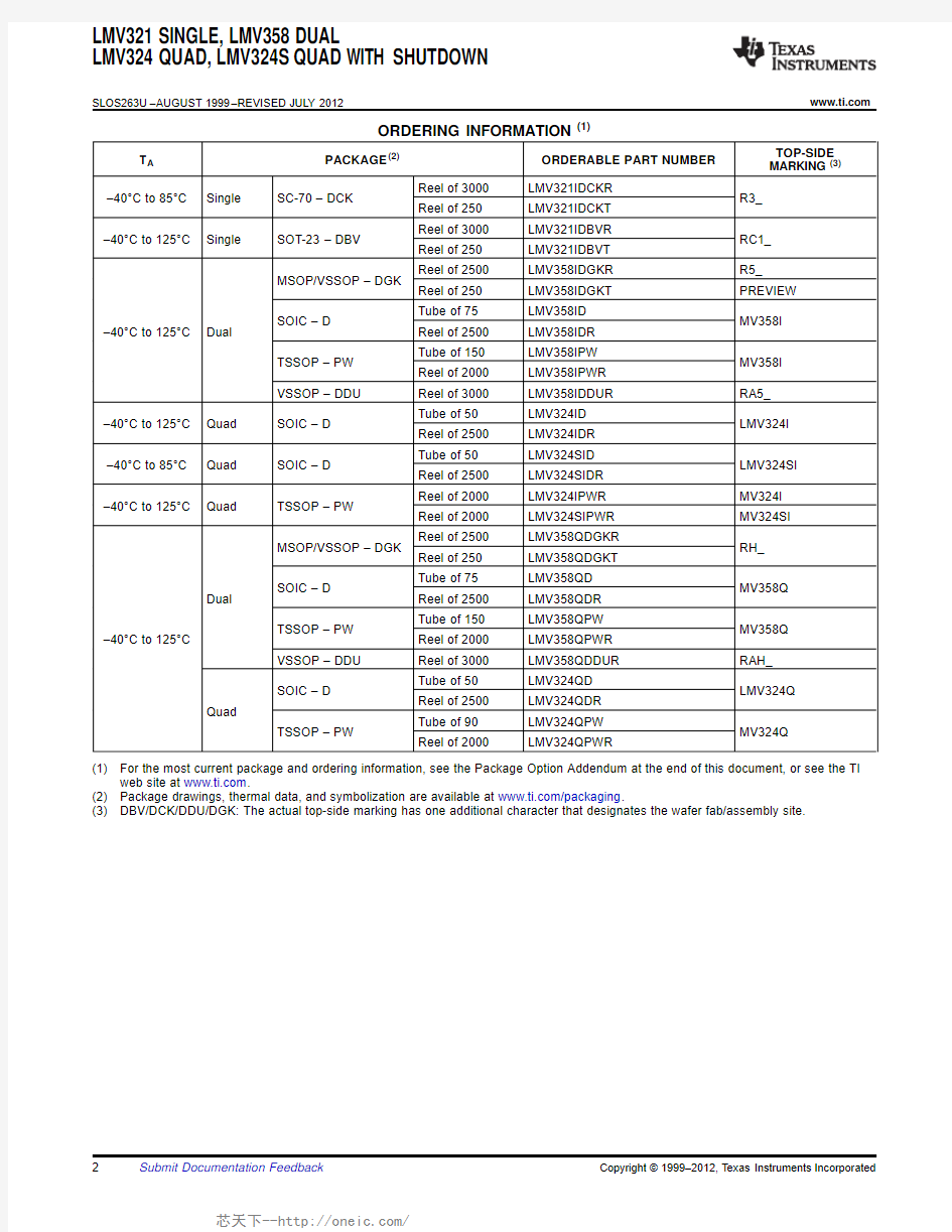
ORDERING INFORMATION(1)
TOP-SIDE T A PACKAGE(2)ORDERABLE PART NUMBER
MARKING(3)
Reel of3000LMV321IDCKR
–40°C to85°C Single SC-70–DCK R3_
Reel of250LMV321IDCKT
Reel of3000LMV321IDBVR
–40°C to125°C Single SOT-23–DBV RC1_
Reel of250LMV321IDBVT
Reel of2500LMV358IDGKR R5_
MSOP/VSSOP–DGK
Reel of250LMV358IDGKT PREVIEW
Tube of75LMV358ID
SOIC–D MV358I
–40°C to125°C Dual Reel of2500LMV358IDR
Tube of150LMV358IPW
TSSOP–PW MV358I
Reel of2000LMV358IPWR
VSSOP–DDU Reel of3000LMV358IDDUR RA5_
Tube of50LMV324ID
–40°C to125°C Quad SOIC–D LMV324I
Reel of2500LMV324IDR
Tube of50LMV324SID
–40°C to85°C Quad SOIC–D LMV324SI
Reel of2500LMV324SIDR
Reel of2000LMV324IPWR MV324I
–40°C to125°C Quad TSSOP–PW
Reel of2000LMV324SIPWR MV324SI
Reel of2500LMV358QDGKR
MSOP/VSSOP–DGK RH_
Reel of250LMV358QDGKT
Tube of75LMV358QD
SOIC–D MV358Q
Dual Reel of2500LMV358QDR
Tube of150LMV358QPW
TSSOP–PW MV358Q
–40°C to125°C Reel of2000LMV358QPWR
VSSOP–DDU Reel of3000LMV358QDDUR RAH_
Tube of50LMV324QD
SOIC–D LMV324Q
Reel of2500LMV324QDR
Quad
Tube of90LMV324QPW
TSSOP–PW MV324Q
Reel of2000LMV324QPWR
(1)For the most current package and ordering information,see the Package Option Addendum at the end of this document,or see the TI
web site at https://www.wendangku.net/doc/ab14047836.html,.
(2)Package drawings,thermal data,and symbolization are available at https://www.wendangku.net/doc/ab14047836.html,/packaging.
(3)DBV/DCK/DDU/DGK:The actual top-side marking has one additional character that designates the wafer fab/assembly site.
2Submit Documentation Feedback Copyright?1999–2012,Texas Instruments Incorporated
IN+
IN-Output
+
–
IN–
IN+
OUT
LMV321SINGLE,LMV358DUAL
LMV324QUAD,LMV324S QUAD WITH SHUTDOWN
https://www.wendangku.net/doc/ab14047836.html,
SLOS263U –AUGUST 1999–REVISED JULY 2012
SYMBOL (EACH AMPLIFIER)
LMV324SIMPLIFIED SCHEMATIC
Copyright ?1999–2012,Texas Instruments Incorporated Submit Documentation Feedback 3
LMV321SINGLE,LMV358DUAL
LMV324QUAD,LMV324S QUAD WITH SHUTDOWN
SLOS263U–AUGUST1999–REVISED https://www.wendangku.net/doc/ab14047836.html, Absolute Maximum Ratings(1)
over operating free-air temperature range(unless otherwise noted)
MIN MAX UNIT
V CC Supply voltage(2) 5.5V
V ID Differential input voltage(3)±5.5V
V I Input voltage range(either input)–0.2 5.5V
At or below T A=25°C,
Duration of output short circuit(one amplifier)to ground(4)Unlimited
V CC≤5.5V
8pin97
D package14pin86
16pin73
DBV package5pin206
DCK package5pin252
θJA Package thermal impedance(5)(6)°C/W
DDU package8pin210
DGK package8pin172
8pin149
PW package14pin113
16pin108
T J Operating virtual junction temperature150°C
T stg Storage temperature range–65150°C (1)Stresses beyond those listed under Absolute Maximum Ratings may cause permanent damage to the device.These are stress ratings
only,and functional operation of the device at these or any other conditions beyond those indicated under Recommended Operating Conditions is not implied.Exposure to absolute-maximum-rated conditions for extended periods may affect device reliability.
(2)All voltage values(except differential voltages and V CC specified for the measurement of I OS)are with respect to the network GND.
(3)Differential voltages are at IN+with respect to IN–.
(4)Short circuits from outputs to V CC can cause excessive heating and eventual destruction.
(5)Maximum power dissipation is a function of T J(max),θJA,and T A.The maximum allowable power dissipation at any allowable ambient
temperature is P D=(T J(max)–T A)/θJA.Operating at the absolute maximum T J of150°C can affect reliability.
(6)The package thermal impedance is calculated in accordance with JESD51-7.
Recommended Operating Conditions(1)
MIN MAX UNIT
V CC Supply voltage(single-supply operation) 2.7 5.5V
V CC=2.7V 1.7
V IH Amplifier turn-on voltage level(LMV324S)(2)V
V CC=5V 3.5
V CC=2.7V0.7
V IL Amplifier turn-off voltage level(LMV324S)V
V CC=5V 1.5
I temperature(LMV321,
–40125
LMV358,LMV324)
T A Operating free-air temperature I temperature(LMV324S,°C
-4085
LMV321IDCK)
Q temperature–40125
(1)All unused control inputs of the device must be held at V CC or GND to ensure proper device operation.See the TI application report,
Implications of Slow or Floating CMOS Inputs,literature number SCBA004.
(2)V IH should not be allowed to exceed V CC.
4Submit Documentation Feedback Copyright?1999–2012,Texas Instruments Incorporated
LMV321SINGLE,LMV358DUAL
LMV324QUAD,LMV324S QUAD WITH SHUTDOWN https://www.wendangku.net/doc/ab14047836.html, SLOS263U–AUGUST1999–REVISED JULY2012 Electrical Characteristics
V CC+=2.7V,T A=25°C(unless otherwise noted)
PARAMETER TEST CONDITIONS MIN TYP(1)MAX UNIT
V IO Input offset voltage 1.77mV
Average temperature coefficient of
αVIO5μV/°C input offset voltage
I IB Input bias current11250nA
I IO Input offset current550nA CMRR Common-mode rejection ratio V CM=0to1.7V5063dB
k SVR Supply-voltage rejection ratio V CC=2.7V to5V,V O=1V5060dB
0–0.2 Common-mode input voltage
V ICR CMRR≥50dB V range 1.9 1.7
High level V CC–100V CC–10
V O Output swing R L=10k?to1.35V mV
Low level60180
LMV321I80170
I CC Supply current LMV358I(both amplifiers)140340μA
LMV324I/LMV324SI(all four amplifiers)260680
B1Unity-gain bandwidth C L=200pF1MHz
Φm Phase margin60deg
G m Gain margin10dB
V n Equivalent input noise voltage f=1kHz46nV/√Hz
I n Equivalent input noise current f=1kHz0.17pA/√Hz
(1)Typical values represent the likely parametric nominal values determined at the time of characterization.Typical values depend on the
application and configuration and may vary over time.Typical values are not ensured on production material.
Shutdown Characteristics(LMV324S)
V CC+=2.7V,T A=25°C(unless otherwise noted)
PARAMETER TEST CONDITIONS MIN TYP(1)MAX UNIT
Supply current in shutdown mode
I CC(SHDN)SHDN≤0.6V5μA
(per channel)
t(on)Amplifier turn-on time A V=1,R L=Open(measured at50%point)2μs
t(off)Amplifier turn-off time A V=1,R L=Open(measured at50%point)40ns (1)Typical values represent the likely parametric nominal values determined at the time of characterization.Typical values depend on the
application and configuration and may vary over time.Typical values are not ensured on production material.
Copyright?1999–2012,Texas Instruments Incorporated Submit Documentation Feedback5
LMV321SINGLE,LMV358DUAL
LMV324QUAD,LMV324S QUAD WITH SHUTDOWN
SLOS263U–AUGUST1999–REVISED https://www.wendangku.net/doc/ab14047836.html, Electrical Characteristics
V CC+=5V,at specified free-air temperature(unless otherwise noted)
PARAMETER TEST CONDITIONS T A(1)MIN TYP(2)MAX UNIT
25°C 1.77
V IO Input offset voltage mV
Full range9 Average temperature
αVIO coefficient of input offset25°C5μV/°C voltage
25°C15250
I IB Input bias current nA
Full range500
25°C550
I IO Input offset current nA
Full range150
Common-mode rejection
CMRR V CM=0to4V25°C5065dB ratio
Supply-voltage V CC=2.7V to5V,V O=1V,
k SVR25°C5060dB rejection ratio V CM=1V
0–0.2 Common-mode input
V ICR CMRR≥50dB25°C V voltage range 4.24
25°C V CC–300V CC–40
High level
Full range V CC–400
R L=2k?to2.5V
25°C120300
Low level
Full range400
V O Output swing mV
25°C V CC–100V CC–10
High level
Full range V CC–200
R L=10k?to2.5V
25°C65180
Low level
Full range280
25°C15100 Large-signal differential
A VD R L=2k?V/mV
voltage gain Full range10
Sourcing,V O=0V560 Output short-circuit
I OS25°C mA
current Sinking,V
=5V10160
O
25°C130250
LMV321I
Full range350
25°C210440
I CC Supply current LMV358I(both amplifiers)μA
Full range615
25°C410830
LMV324I/LMV324SI
(all four amplifiers)Full range1160
B1Unity-gain bandwidth C L=200pF25°C1MHz
Φm Phase margin25°C60deg
G m Gain margin25°C10dB
Equivalent input
V n f=1kHz25°C39nV/√Hz noise voltage
Equivalent input
I n f=1kHz25°C0.21pA/√Hz
noise current
SR Slew rate25°C1V/μs (1)Full range T A=–40°C to125°C for I temperature(LMV321,LMV358,LMV324),–40°C to85°C for(LMV324S,LMV321IDCK)and–40°C
to125°C for Q temperature.
(2)Typical values represent the likely parametric nominal values determined at the time of characterization.Typical values depend on the
application and configuration and may vary over time.Typical values are not ensured on production material.
6Submit Documentation Feedback Copyright?1999–2012,Texas Instruments Incorporated
LMV321SINGLE,LMV358DUAL
LMV324QUAD,LMV324S QUAD WITH SHUTDOWN https://www.wendangku.net/doc/ab14047836.html, SLOS263U–AUGUST1999–REVISED JULY2012 Shutdown Characteristics(LMV324S)
V CC+=5V,T A=25°C(unless otherwise noted)
PARAMETER TEST CONDITIONS MIN TYP(1)MAX UNIT
Supply current in shutdown mode
I CC(SHDN)SHDN≤0.6V,T A=Full Temperature Range5μA
(per channel)
t(on)Amplifier turn-on time A V=1,R L=Open(measured at50%point)2μs
t(off)Amplifier turn-off time A V=1,R L=Open(measured at50%point)40ns
(1)Typical values represent the likely parametric nominal values determined at the time of characterization.Typical values depend on the
application and configuration and may vary over time.Typical values are not ensured on production material.
Copyright?1999–2012,Texas Instruments Incorporated Submit Documentation Feedback7
Phase Margin ? Deg
G a i n ? d B LMV321 FREQUENCY RESPONSE
vs
Frequency ? Hz
Phase Margin ? Deg
G a i n ? d B LMV321 FREQUENCY RESPONSE
vs
Frequency ? Hz
Phase Margin ? Deg G a i n ? d B
LMV321 FREQUENCY RESPONSE
vs
Frequency ? Hz
Phase Margin ? Deg
LMV321 FREQUENCY RESPONSE
vs
Frequency ? Hz
G a i n ? d B
LMV321SINGLE,LMV358DUAL
LMV324QUAD,LMV324S QUAD WITH SHUTDOWN
SLOS263U –AUGUST 1999–REVISED JULY 2012
https://www.wendangku.net/doc/ab14047836.html,
TYPICAL CHARACTERISTICS
Figure 1.Figure 2.
Figure 3.Figure 4.
8Submit Documentation Feedback Copyright ?1999–2012,Texas Instruments Incorporated
C a p a c i t i v e L o a d ? n F
STABILITY
vs
Output Voltage ? V
C a p a c i t i v e L o a d ? p F
STABILITY
vs
Phase Margin ? Deg
LMV321 FREQUENCY RESPONSE
vs
Frequency ? Hz
G a i n ? d B
Output Voltage ? V
C a p a c i t i v e L o a d ? p F STABILITY
vs
CAPACITIVE LOAD
LMV321SINGLE,LMV358DUAL
LMV324QUAD,LMV324S QUAD WITH SHUTDOWN
https://www.wendangku.net/doc/ab14047836.html,
SLOS263U –AUGUST 1999–REVISED JULY 2012
TYPICAL CHARACTERISTICS (continued)
Figure 5.Figure 6.
Figure 7.Figure 8.
Copyright ?1999–2012,Texas Instruments Incorporated Submit Documentation Feedback 9
I n p u t C u r r e n t ? n A
INPUT CURRENT
vs
SUPPLY CURRENT
vs
S u p p l y C u r
r e n t ? A
μ
STABILITY
vs
C a p a c i t i v e L o a d ? n F
? Supply Voltage ? V
S l e w R a t e ? V /SLEW RATE
vs
μs
V CC LMV321SINGLE,LMV358DUAL
LMV324QUAD,LMV324S QUAD WITH SHUTDOWN
SLOS263U –AUGUST 1999–REVISED JULY 2012
https://www.wendangku.net/doc/ab14047836.html,
TYPICAL CHARACTERISTICS (continued)
Figure 9.Figure 10.
Figure 11.Figure 12.
10Submit Documentation Feedback Copyright ?1999–2012,Texas Instruments Incorporated
S i n k i n g C u r r e n t ? m
A
SINKING CURRENT
vs
S i n k i n g C u r r e n t ? m A
SINKING CURRENT
vs
S o u r c i n g C u r r e n t ? m A
SOURCE CURRENT
vs
S o u r c i n g C u r r e n t ? m A
SOURCE CURRENT
vs
LMV321SINGLE,LMV358DUAL
LMV324QUAD,LMV324S QUAD WITH SHUTDOWN
https://www.wendangku.net/doc/ab14047836.html,
SLOS263U –AUGUST 1999–REVISED JULY 2012
TYPICAL CHARACTERISTICS (continued)
Figure 13.Figure 14.
Figure 15.Figure 16.
Copyright ?1999–2012,Texas Instruments Incorporated Submit Documentation Feedback 11
+k SVR vs
+k
S V R ? d B
?k SVR vs
?k S V R ? d B
SHORT-CIRCUIT CURRENT
vs
S i n k i n g C u r r e n t ? m A
SHORT-CIRCUIT CURRENT
vs
S o u r c i n g C u r r e n t ? m A
LMV321SINGLE,LMV358DUAL
LMV324QUAD,LMV324S QUAD WITH SHUTDOWN
SLOS263U –AUGUST 1999–REVISED JULY 2012
https://www.wendangku.net/doc/ab14047836.html,
TYPICAL CHARACTERISTICS (continued)
Figure 17.Figure 18.
Figure 19.Figure 20.
12Submit Documentation Feedback Copyright ?1999–2012,Texas Instruments Incorporated
O u t p u t V o l t a g e S w i n g ? m V
OUTPUT VOLTAGE SWING FROM RAILS
vs
OUTPUT VOLTAGE
vs
P e a k O u t p u t V o l t a g e ? V Frequency ? Hz
O P
P
?k SVR vs
?k S V R ? d B
+k S V R +k SVR vs
? d B
LMV321SINGLE,LMV358DUAL
LMV324QUAD,LMV324S QUAD WITH SHUTDOWN
https://www.wendangku.net/doc/ab14047836.html,
SLOS263U –AUGUST 1999–REVISED JULY 2012
TYPICAL CHARACTERISTICS (continued)
Figure 21.Figure 22.
Figure 23.Figure 24.
Copyright ?1999–2012,Texas Instruments Incorporated Submit Documentation Feedback 13
NONINVERTING LARGE-SIGNAL
NONINVERTING LARGE-SIGNAL
C r o s s t a l k R e j e c t i o n ? d B
CROSSTALK REJECTION
vs
I m p e d a n c e ?OPEN-LOOP OUTPUT IMPEDANCE
vs
?
LMV321SINGLE,LMV358DUAL
LMV324QUAD,LMV324S QUAD WITH SHUTDOWN
SLOS263U –AUGUST 1999–REVISED JULY 2012
https://www.wendangku.net/doc/ab14047836.html,
TYPICAL CHARACTERISTICS (continued)
Figure 25.Figure 27.Figure 28.
14Submit Documentation Feedback Copyright ?1999–2012,Texas Instruments Incorporated
NONINVERTING SMALL-SIGNAL
NONINVERTING SMALL-SIGNAL
50 m V /D i v
NONINVERTING LARGE-SIGNAL
NONINVERTING SMALL-SIGNAL
LMV321SINGLE,LMV358DUAL
LMV324QUAD,LMV324S QUAD WITH SHUTDOWN
https://www.wendangku.net/doc/ab14047836.html,
SLOS263U –AUGUST 1999–REVISED JULY 2012
TYPICAL CHARACTERISTICS (continued)
Figure 29.Figure 30.
Figure 31.Figure 32.
Copyright ?1999–2012,Texas Instruments Incorporated Submit Documentation Feedback 15
INVERTING SMALL-SIGNAL
PULSE RESPONSE
INVERTING LARGE-SIGNAL
INVERTING LARGE-SIGNAL
INVERTING LARGE-SIGNAL
LMV321SINGLE,LMV358DUAL
LMV324QUAD,LMV324S QUAD WITH SHUTDOWN
SLOS263U –AUGUST 1999–REVISED JULY 2012
https://www.wendangku.net/doc/ab14047836.html,
TYPICAL CHARACTERISTICS (continued)
Figure 33.Figure 34.
Figure 35.Figure 36.
16Submit Documentation Feedback Copyright ?1999–2012,Texas Instruments Incorporated
I n p u t C u r r e n t N o i s e ? p A /INPUT CURRENT NOISE
vs
H z
I n p u t C u r r e n t N o i s e ? p A /INPUT CURRENT NOISE
vs
H z
INVERTING SMALL-SIGNAL
PULSE RESPONSE
50 m V /D i v
INVERTING SMALL-SIGNAL
LMV321SINGLE,LMV358DUAL
LMV324QUAD,LMV324S QUAD WITH SHUTDOWN
https://www.wendangku.net/doc/ab14047836.html,
SLOS263U –AUGUST 1999–REVISED JULY 2012
TYPICAL CHARACTERISTICS (continued)
Figure 37.Figure 38.
Figure 39.Figure 40.
Copyright ?1999–2012,Texas Instruments Incorporated Submit Documentation Feedback 17
THD + N vs
T H D ? %
THD + N vs
T H D ?
%
INPUT VOLTAGE NOISE
vs
I n p u t V o l t a g e N o i s e ? n V /H
z
THD + N vs
T H D ? %
LMV321SINGLE,LMV358DUAL
LMV324QUAD,LMV324S QUAD WITH SHUTDOWN
SLOS263U –AUGUST 1999–REVISED JULY 2012
https://www.wendangku.net/doc/ab14047836.html,
TYPICAL CHARACTERISTICS (continued)
Figure 41.Figure 42.
Figure 43.Figure 44.
18Submit Documentation Feedback Copyright ?1999–2012,Texas Instruments Incorporated
THD + N vs
T H D ? %
LMV321SINGLE,LMV358DUAL
LMV324QUAD,LMV324S QUAD WITH SHUTDOWN
https://www.wendangku.net/doc/ab14047836.html,
SLOS263U –AUGUST 1999–REVISED JULY 2012
TYPICAL CHARACTERISTICS (continued)
Figure 45.
Copyright ?1999–2012,Texas Instruments Incorporated Submit Documentation Feedback 19
LMV321SINGLE,LMV358DUAL
LMV324QUAD,LMV324S QUAD WITH SHUTDOWN
SLOS263U–AUGUST1999–REVISED https://www.wendangku.net/doc/ab14047836.html,
REVISION HISTORY
Changes from Revision T(September2007)to Revision U Page ?UpdatedθJA value for DDU package (4)
20Submit Documentation Feedback Copyright?1999–2012,Texas Instruments Incorporated