AN-4140_Transformer Design Consideration

Application Note AN4140
Transformer Design Consideration for off-line Flyback Converters using Fairchild Power Switch (FPS TM )
https://www.wendangku.net/doc/a018653024.html,
Rev. 1.0.0
1. Introduction
For flyback coverters, the transformer is the most important factor that determines the performance such as the efficiency, output regulation and EMI. Contrary to the normal transformer, the flyback transformer is inherently an inductor that provides energy storage, coupling and isolation for the flyback converter. In the general transformer, the current flows in both the primary and secondary winding at the same time. However, in the flyback transformer, the current flows only in the primary winding while the energy in the core is charged and in the secondary winding while the energy in the core is discharged. Usually gap is introduced between the core to increase the energy storage capacity. This paper presents practical design considerations of transformers for off-line flyback converters employing Fairchild Power Switch (FPS). In order to give insight to the reader, practical design examples are also provided.
2. General Transformer design procedure
(1) Choose the proper core
Core type : Ferrite is the most widely used core material for commercial SMPS (Switchied mode power supply)applications. Various ferrite cores and bobbins are shown in Figure 1. The type of the core should be chosen with regard to system requirements including number of outputs,physical height, cost and so on. Table 1 shows features and typical application of various cores.
Figure 1. Ferrite core (TDK)
Table 1. Features and typical applications of various cores
Core size : Actually, the initial selection of the core is bound to be crude since there are too many variables. One way to select the proper core is to refer to the manufacture's core selection guide. If there is no proper reference, use the table 2 as a starting point. The core recommended in table 1is typical for the universal input range, 67kHz switching frequency and 12V single output application. When the input voltage range is 195-265 Vac (European input range) or the switching frequency is higher than 67kHz, a smaller core can be used. For an application with low voltage and/or multiple outputs, usually a larger core should be used than recommended in the table.
Table 2. Core quick selection table (For universal input range, fs=67kHz and 12V single output)
Core Features Typical Applications EE EI -Low cost Aux. power Battery charger EFD EPC -Low profile
LCD Monitor EER
-Large winding window area -Various bobbins for multiple output
CRT monitor, C-TV DVDP, STB
PQ
-Large cross sectional area -Relatively expensive
Output Power EI core EE core EPC core EER core
0-10W
EI12.5EI16EI19EE8EE10EE13EE16EPC10EPC13EPC1710-20W EI22EE19EPC1920-30W EI25EE22EPC25EER25.530-50W EI28EI30EE25EPC30
EER2850-70W EI35EE30EER28L 70-100W
EI40
EE35EER35100-150W EI50EE40EER40EER42150-200W EI60
EE50EE60
EER49
AN4140APPLICATION NOTE
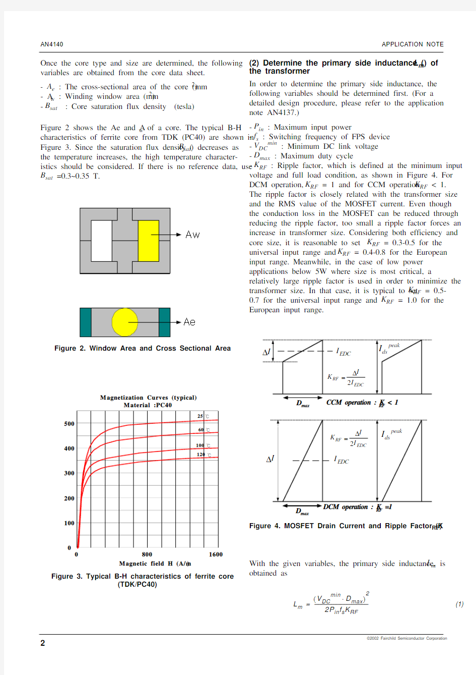
Once the core type and size are determined, the following variables are obtained from the core data sheet.
- A e : The cross-sectional area of the core (mm2)
- A w : Winding window area (mm2)
- B sat : Core saturation flux density (tesla)
Figure 2 shows the Ae and A w of a core. The typical B-H characteristics of ferrite core from TDK (PC40) are shown in Figure 3. Since the saturation flux density (B sat) decreases as the temperature increases, the high temperature character-istics should be considered. If there is no reference data, use B sat =0.3~0.35 T.
Figure 2. Window Area and Cross Sectional Area
Figure 3. Typical B-H characteristics of ferrite core
(TDK/PC40) (2) Determine the primary side inductance (L m) of the transformer
In order to determine the primary side inductance, the following variables should be determined first. (For a detailed design procedure, please refer to the application note AN4137.)
- P in : Maximum input power
- f s : Switching frequency of FPS device
- V DC min : Minimum DC link voltage
- D max : Maximum duty cycle
- K RF : Ripple factor, which is defined at the minimum input voltage and full load condition, as shown in Figure 4. For DCM operation, K RF = 1 and for CCM operation K RF < 1. The ripple factor is closely related with the transformer size and the RMS value of the MOSFET current. Even though the conduction loss in the MOSFET can be reduced through reducing the ripple factor, too small a ripple factor forces an increase in transformer size. Considering both efficiency and core size, it is reasonable to set K RF = 0.3-0.5 for the universal input range and K RF = 0.4-0.8 for the European input range. Meanwhile, in the case of low power applications below 5W where size is most critical, a relatively large ripple factor is used in order to minimize the transformer size. In that case, it is typical to set K RF = 0.5-0.7 for the universal input range and K RF = 1.0 for the European input range.
Figure 4. MOSFET Drain Current and Ripple Factor (K RF)
With the given variables, the primary side inductance, L m is obtained as
L m
V DC min D max
?
()2
2P in f s K RF
---------------------------------------------
= (1)
APPLICATION NOTE AN4140
where V DC min is the minimum DC input voltage, D max is the maximum duty cycle, P in is the maximum input power , f s is the switching frequency of the FPS device and K RF is the ripple factor.
Once L m is determined, the maximum peak current and RMS current of the MOSFET in normal operation are obtained as
With the chosen core, the minimum number of turns for the transformer primary side to avoid the core saturation is given by
where L m is the primary side inductance, I over is the FPS
pulse-by-pulse current limit level, A e is the cross-sectional area of the core and B sat is the saturation flux density in tesla.
If the pulse-by-pulse current limit level of FPS is larger than the peak drain current of the power supply design, it may result in excessive transformer size since I over is used in determining the minimum primary side turns as shown in equation (6). Therefore, it is required to choose a FPS with proper current limit specifications or to adjust the peak drain current close to I over by increasing the ripple factor as shown in Figure 5. It is reasonable to design I ds peak to be 70-80% of I over considering the transient response and tolerance of I over .
Figure 5. Adjustment peak drain current
(3) Determine the number of turns for each output Figure 6 shows the simplified diagram of the transformer,whrere V o1 stands for the reference output that is regulated by the feedback control while V o(n) stands for the n-th output.
First, determine the turns ratio (n) between the primary side and the feedback controlled secondary side as a reference.
where N p and N s1 are the number of turns for primary side and reference output, respectively, V o1 is the output voltage and V F1 is the diode (D R1) forward voltage drop of the reference output that is regulated by the feedback control.Then, determine the proper integer for N s1 so that the resulting Np is larger than N p min obtained from equation (6). The number of turns for the other output (n-th output) is determined as
The number of turns for Vcc winding is determined as
where V cc * is the nominal value of the supply voltage of the FPS device, and V Fa is the forward voltage drop of D a as defined in Figure 6. Since V cc increases as the output load increases, it is proper to set V cc * as V cc start voltage (refer to the data sheet) to avoid triggering the over voltage protection during normal operation.
Figure 6. Simplified diagram of the transformer
I ds peak
I EDC ?I
2-----+= (2) I ds
rms
3I EDC ()2
?I 2-----
2
+D max 3
-------------=
3()
where
I EDC P in
V DC min D max ?-------------------------------------=4()
and ?I V DC min
D max
L m f s
-----------------------------------= (5)
N P
min
L m I over B sat A e
------------
-------106
(turns)×= (6)
n V R0
V o1V F1+-------------------------N P N s1
---------== (7)
N s n ()V o n ()V F n ()
+V o1V F1
+---------------------------------=N s1?turns ()
8()
N a V cc *V Fa
+V o1V F1
+---------------------------
=N s1?turns ()
9()
AN4140APPLICATION NOTE
Once the number of turns on the primary side have been determined, the gap length of the core is obtained through approximation as
where A L is the AL-value with no gap in nH/turns 2, Ae is the cross sectional area of the core as shown in Figure 2, L m is specified in equation (1) and N p is the number of turns for the primary side of the transformer
(4) Determine the wire diameter for each winding
The wire diameter is determined based on the rms current through the wire. The current density is typically 5A/mm 2when the wire is long (>1m). When the wire is short with a small number of turns, a current density of 6-10 A/mm 2 is also acceptable. Avoid using wire with a diameter larger than 1 mm to avoid severe eddy current losses as well as to make winding easier. For high current output, it is better to use parallel windings with multiple strands of thinner wire to minimize skin effect.
3. Transformer Construction Method.
(1) Winding Sequence (a) Primary winding
Figure 7. Primary side winding
It is typical to place all the primary winding or a portion of the primary winding innermost on the bobbin. This minimizes the length of wire, reducing the conduction loss in the wire. The EMI noise radiation can be reduced, since the other windings can act as Faraday shields. When the primary side winding has more than two layers, the innermost layer winding should start from the drain pin of FPS as shown in Figure 7. This allows the winding driven by the highest voltage to be shielded by other windings, thereby maximizing the shielding effect. (b) Vcc winding
In general, the voltage of each winding is influenced by the voltage of the adjacent winding. The optimum placement of the Vcc winding is determined by the over voltage protection (OVP) sensitivity, the Vcc operating range and control scheme.
-Over voltage protection (OVP) sensitivity : When the output voltage goes above its normal operation value due to some abnormal situation, Vcc voltage also increases. FPS uses Vcc voltage to indirectly monitor the over voltage situation in the secondary side. However, a RCD snubber network acts as an another output as shown in Figure 8 and Vcc voltage is also influenced by the snubber capacitor voltage. Because the snubber voltage increases as the drain current increases, OVP of FPS can be triggered not only by the output over voltage condition, but also by the over load condition.
The sensitivity of over voltage protection is closely related to the physical distance between windings. If the Vcc winding is close to the secondary side output winding, Vcc voltage will change sensitively to the variation of the output voltage.Meanwhile, if the Vcc winding is placed close to the primary side winding, Vcc voltage will vary sensitively as the snubber capacitor voltage changes.
Figure 8. Primary side winding
G 40πA e N P 2
1000L m --------------------1A L ------–
=mm ()10(
)
APPLICATION NOTE AN4140
- Vcc operating range : As mentioned above, Vcc voltage is influenced by the snubber capacitor voltage. Since the snubber capacitor voltage changes according to drain current, Vcc voltage can go above its operating range triggering OVP in normal operation. In that case, Vcc winding should be placed closest to the reference output winding that is regulated by feedback control and far from the primary side winding as shown in Figure 9.
Figure 9. Winding sequence to reduce Vcc variation
- Control scheme : In the case of primary side regulation,the output voltages should follow the Vcc voltage tightly for a good output regulation. Therefore, Vcc winding should be placed close to the secondary windings to maximize the coupling of the Vcc winding with the secondary windings.Meanwhile, Vcc winding should be placed far from primary winding to minimize coupling to the primary. In the case of secondary side regulation, the Vcc winding can be placed between the primary and secondary or on the outermost position.
(c) Secondary side winding
When it comes to a transformer with multiple outputs, the highest output power winding should be placed closest to the primary side winding, to reduce leakage inductance and to maximize energy transfer efficiency. If a secondary side winding has relatively few turns, the winding should be spaced to traverse the entire width of the winding area for improved coupling. Using multiple parallel strands of wire will also help to increase the fill factor and coupling for the secondary windings with few turns as shown in Figure 10.To maximize the load regulation, the winding of the output with tight regulation requirement should be placed closest to the winding of the reference output that is regulated by the feedback control.
Figure 10. Multiple parallel strands winding
(2) Winding method
-Stacked winding on other winding: A common technique for winding multiple outputs with the same polarity sharing a common ground is to stack the secondary windings instead of winding each output winding separately, as shown in Figure 11. This approach will improve the load regulation of the stacked outputs and reduce the total number of secondary turns. The windings for the lowest voltage output provide the return and part of the winding turns for the next higher voltage output. The turns of both the lowest output and the next higher output provide turns for succeeding outputs. The wire for each output must be sized to accommodate its output current plus the sum of the output currents of all the output stacked on top of it.
-Stacked winding on other output: If a transformer has a very high voltage and low current output, the winding can be stacked on the lower voltage output as shown in Figure 12.This approach provides better regulation and reduced diode voltage stress for the stacked output. The wire and rectifier diode for each output must be sized to accommodate its output current plus the sum of the output currents of all the output stacked on top of it.
Figure 11. Stacked winding on other winding
Figure 12. Stacked winding on other output
(3) Minimization of Leakage Inductance
The winding order in a transformer has a large effect on the leakage inductance. In a multiple output transformer, the secondary with the highest output power should be placed closest to the primary for the best coupling and lowest leakage. The most common and effective way to minimize the leakage inductance is a sandwich winding as shown in Figure 13. Secondary windings with only a few turns should be spaced across the width of the bobbin window instead of being bunched together, in order to maximize coupling to the primary. Using multiple parallel strands of wire is an additional technique of increasing the fill factor and coupling of a winding with few turns as shown in Figure 10.
Figure 13. Sandwich winding
(4) Transformer shielding
A major source of common mode EMI in Switched Mode Power Supply (SMPS) is the parasitic capacitances coupled to the switching devices. The MOSFET drain voltage drives capacitive current through various parasitic capacitances. Some portion of these capacitive currents flow into the neutral line that is connected to the earth ground and observed as common mode noise. By using an electrostatic separation shield between the windings (at primary winding side, or at secondary winding side, or both), the common mode signal is effectively "shorted" to the ground and the capacitive current is reduced. When properly designed, such shielding can dramatically reduce the conducted and radiated emissions and susceptibility. By using this technique, the size of EMI filter can be reduced. The shield can be easily implemented using copper foil or tightly wound wire. The shield should be virtually grounded to a quiescent point such as primary side DC link, primary ground or secondary ground.
Figure 14 shows a shielding example, which allows the removal of the Y-capacitor that is commonly used to reduce common mode EMI. As can be seen, shields are used not only on the bottom but also on the top of the primary winding in order to cancel the coupling of parasitic capaci-tances. Figure 15 also shows the detailed shielding construction.
Figure 14. Shielding example to remove Y-capacitor (5) Practical examples of transformer construction
As described in the above sections, there many factors that should be considered in determining the winding sequence and winding method. In this section some practical examples of transformer construction are presented to give a compre-hensive understanding of practical transformer construction.
Figure 15. Shielding method to remove Y-Capacitor
a) LCD monitor SMPS example
Figure 16 shows a simplified transformer schematic for typical LCD monitor SMPS. The 5V output is for the Micro-processor and 13V output is for the inverter input of LCD back light. While 5V output is regulated with the feedback control, 13V output is determined by the transformer turns ratio and a stacked winding is usually used to maximize the regulation.
Transformer construction Example A (Figure 17) : In this example, the leakage inductance is minimized by employing a sandwich winding. The Vcc winding is placed outside to provide shielding effect. Since the Vcc winding is placed on the top half of primary winding, the coupling between the Vcc winding and 5V output winding is poor, which may require a small dummy load on the 5V output to prevent UVLO (Under V oltage Lock Out) in the no load condition. Transformer construction Example B (Figure 18) : In this example, the leakage inductance is larger than example A, since a sandwich winding is not used. However, the Vcc winding is tightly coupled with the 5V output winding and Vcc remains its normal operation range in the no load condition. Even though this approach can prevent UVLO in no load conditions without dummy load, the power conversion efficiency might be relatively poor compared to example A due to the large leakage inductance.
Figure 16. LCD monitor SMPS transformer example Figure 17. LCD monitor SMPS transformer construction example (A)Figure 18. LCD monitor SMPS transformer construction example (B)
(b) CRT monitor SMPS example - PSR (Primary side regulation)
Figure 19 shows a simplified transformer schematic for a typical CRT monitor SMPS employing PSR (Primary side regulation). 80V and 50V outputs are the main output having high output power. Meanwhile, 5V and 6.5V outputs are auxiliary output having small output power. The 80V output winding is stacked on the 50V output to reduce the voltage stress of the rectifier diode (D R1).
Figure 19. CRT monitor SMPS transformer example-PSR
Figure 20 shows the detailed transformer construction. In order to minimize the leakage inductance, sandwich winding is employed and the main output windings are placed closest to the primary winding. The Vcc winding is placed closest to the main output windings to provide tight regulations of the main output. The auxiliary output windings are placed outside of the primary winding to provide a shielding effect.
Figure 20. CRT monitor SMPS transformer construction example (PSR)
(c) CRT monitor SMPS example - SSR (Secondary side regulation)
Figure 21 shows a simplified transformer schematic for typical CRT monitor SMPS employing SSR (Secondary side regulation). 80V and 50V outputs are the main output having high output power. Meanwhile, 5V and 6.5V outputs are auxiliary output having small output power. The 80V output winding is stacked on 50V output to reduce the voltage stress of the rectifier diode (D R1).
Figure 22 shows the detailed transformer construction. In order to minimize the leakage inductance, a sandwich winding is employed and the main output windings are placed closest to the primary winding. The Vcc winding is placed outermost to provide a shielding effect. The auxiliary output windings are placed between windings of the main output winding to obtain better regulation.
Figure 21. CRT monitor SMPS transformer example-SSR
Figure 22. CRT monitor SMPS transformer construction example (SSR)
References
Colonel Wm. T. McLyman, Transformer and Inductor design Handbook, 2nd ed. Marcel Dekker, 1988.
Anatoly Tsaliovich, Electromagnetic shielding handbook for wired and wireless EMC application, 1998
Bruce C. Gabrielson and Mark J. Reimold, "Suppression of Powerline noise with isolation transformers", EMC expo87 San Diego, 1987.
D.Cochrane, D.Y.Chen, D. Boroyevich, "Passive cancel-lation of common mode noise in power electronics circuits," PESC 2001, pp.1025-1029
Otakar A. Horna, "HF Transformer with triaxial cable shielding against capacitive current", IEEE Transactions on parts, hybrids, and packaging, vol.php-7, N0.3 , Sep. 1971.
DISCLAIMER
FAIRCHILD SEMICONDUCTOR RESERVES THE RIGHT TO MAKE CHANGES WITHOUT FURTHER NOTICE TO ANY PRODUCTS HEREIN TO IMPROVE RELIABILITY, FUNCTION OR DESIGN. FAIRCHILD DOES NOT ASSUME ANY
LIABILITY ARISING OUT OF THE APPLICATION OR USE OF ANY PRODUCT OR CIRCUIT DESCRIBED HEREIN; NEITHER DOES IT CONVEY ANY LICENSE UNDER ITS PATENT RIGHTS, NOR THE RIGHTS OF OTHERS.
LIFE SUPPORT POLICY
FAIRCHILD’S PRODUCTS ARE NOT AUTHORIZED FOR USE AS CRITICAL COMPONENTS IN LIFE SUPPORT DEVICES OR SYSTEMS WITHOUT THE EXPRESS WRITTEN APPROVAL OF THE PRESIDENT OF FAIRCHILD SEMICONDUCTOR CORPROATION. As used herein:
1.Life support devices or systems are devices or systems
which, (a) are intended for surgical implant into the body, or (b) support or sustain life, or (c) whose failure to perform when properly used in accordance with instructions for use provided in the labeling, can be reasonably expected to result in significant injury to the user.
2. A critical component is any component of a life support
device or system whose failure to perform can be
reasonably expected to cause the failure of the life support device or system, or to affect its safety or effectiveness.
https://www.wendangku.net/doc/a018653024.html,
by Hang-Seok Choi / Ph. D
Power Supply Group / Fairchild Semiconductor
Phone : +82-32-680-1383 Facsimile : +82-32-680-1317E-mail : hschoi@fairchildsemi.co.kr
面相中的十大凶相都有这些,你知道吗,看完该注意了
面相中的十大凶相都有这些,你知道吗,看完该注意了 谓的面相‘五官’,指的就是‘耳、眉、眼、鼻、口’等五种人体器官。面相就是一个人所具有的独特气质,而成为形或色表现于面上,给人的一种感受。接下来为大家详细介绍面相算命图解大全。面相可分为三庭看,人的眉以上是上庭,人的眉至鼻头是中庭,人的鼻头以下就为下庭。面部三庭要均匀。即额头、眉眼鼻、嘴与下巴的比例要均匀,整个面部显得大方磊落。若是额形生得略高阔饱满,则代表少年运佳,但额不能太高,过高会克夫,太低则少年运差,当然没法早嫁。在面部五官之后,再细分便是十二宫。这十二个宫位囊括了面部所有的特性和吉凶。第一宫:命宫,又为愿望之宫。麻衣曰:其居两眉间,山根之上,为印堂。第二宫:财帛宫,位于土宿,包括天仓、地库、金甲、井灶。主察财运。第三宫:兄弟宫,又称交友宫。麻衣曰:位居两眉。主交友运。第四宫:田宅宫,田宅宫,位于两眼,及上眼睑。主家业运第五宫:男女宫,又称子女宫。麻衣曰:位于两眼之下,又称为泪堂。看子嗣运。第六宫:奴仆宫,麻衣说它位居地阁,重接水星。看管理运。第七宫:妻妾宫,也可以称为夫妻宫,就在眼尾。第八宫:疾厄宫,一说是山根位,一说是年寿位,建议以鼻梁统看。第九宫:迁移宫,迁移者,位居眉角。古相士,以迁移宫的位置看人阴阳宅状况。第十宫:官禄宫,
官禄者,为居中正,上合离宫。反应人的禄命官运。第十一宫:福德宫,福德者,位居天仓,牵连地阁。看福禄之运。第十二宫:父母宫,便是额头的日月角。主看父母的福祸疾厄。看面相,形体外貌、精神气质、举止情态皆可一视而察,情人、恋人、夫妻、同事、朋友之间、感情总会有变化的、是相互信任、倾慕也可以从面相看出来。额头眉毛之间只有一道纵纹。这种面相在相学中被称为天柱纹。有此面相的人个性都很顽强。是属于做事不达目的绝不会放弃,对利益也是分得很清楚。一般来讲他们是不做对自己无利的事情。这样的人不但严以律己。同时对别人的要求也非常严格。但还有就是是这种面相的人有一个特征,那就好是这道纵纹平时是不会出现。当他的身心俱疲的时候,这道皱纹才会出现。鼻子的上部这些部位若是出现了数条横纹的人。有此面相特征者对事物都会表现出十足的热情。甚至可以说是充满激情。不仅是做事情又积极又主动。待人处事也是持着一颗平常心。此外,如果是说笑时出现这种皱纹的人。一般性格都是较为温和。缺点就是比较好管别人的事情。也常常为此惹祸上身。 1、男人的眉毛中间稀疏杂乱、毛形逆生,是为乱性之相, 情绪十分不稳定,伴有较重的暴力倾向。-2、双眉过低而压眼,是为心性阴沉扭曲而走极端。-3、女子眉过粗浓,不仅一生婚姻难成,且有妨夫。-4、印堂过窄小,难容两指的人,一生运势不顺且多灾厄。-5、女子双颧露骨而突起,对夫运
14种鼻型图解
26种面型算命图解 侧面观察 1、凸面型 上停位居前额,代表十五至三十岁、父母缘分、思想智慧等事。从侧面观看,这种面型的额头是向后倾斜,表示思想敏捷,下巴向后退缩,不是行动迅速。 但一个人思想、行动都迅速,则其人是一个容易冲动的人 2、凹面型 这种面型的人额头与下巴皆凸出,形成中央鼻子部位凹入 这种人思想、行动都慢;但有忍耐力,不会轻易冲动,给人感觉城府很深,不轻易向他人吐露心声。 3、直面型 直面形是前额与下巴皆没有凸出或退缩,这种面型的人思想与行动都不会急躁或太慢,做任何事都会按部就班,从容面对。 4、额凸下巴退缩 额凸代表思想慢,下巴退缩则代表行动快。 这种面相的人思想慢而行动快,其行动往往未经深思熟虑,所以常有错误的抉择。 5、额斜下巴凸
额斜是思想迅速,下巴凸出是行动缓慢,这种人碰到任何问题都会立即得到思想是回应,但不会马上行动,而会慢慢地行动,大部分人都是这种下巴。 正面观察 正面观察面型的方法较侧面多,有西洋骨相学的三分法,中国的五分法、十分法 其实三分法与五分有许多相同之处,三分法是以人类的思想、行动、物欲享受划分种类,而十分法只是把三分发再细致分划为十种。 三分法 1、思想型 思想型的人其特点是上额广阔而高,下巴尖而小,形成一个倒三角形。 这种形格的人身材一般都属细小、腰部狭窄、手一般略长、面色带白、头发幼而密。 「思想型」这正是推动他们走向成功之路的因素;所以很多科学家、研究家在未成功之前常常会给人行为疯狂、不切实际之感觉。 这种形格的人适宜做科学研究、教育、建筑师、设计师或数学家、分析家等工作。 2、运动型
运动型的人特点就是颧骨高耸,鼻形长而鼻梁有节,腮骨显露,前额一般较低而额上有横纹、面色带黑、头发粗而多、身材高大强壮。其性格特点是忍耐力强,有冒险精神,有责任心,敢作敢为,刻苦耐劳。 这种面型的人最适合从事劳动工作,如工程师、冒险家、探险家、军人、警察或运动员等 3、享受型 享受型的人其特点是颐部园肥,前额较窄小,形成一个正三角形或圆形的面。鼻形较小,鼻头园而有肉,头发幼而疏,面色略微带红,手脚较短,脸部特别肥大,肉多骨少。 这种人处事圆滑,交际手腕强。这种人最适合经商 以上三种形质,只是基本形而已。因为每一个人同样会兼有思想型、运动型及享受型的特征,只是多寡而已,但最好是三种形质发展平衡,这样可工作不忘娱乐,娱乐不忘工作。 如果思想型过重的话,这种人每天只是充满幻想,不肯面对现实,容易引发神经衰落及头痛病等病症,如果再加上整个脸型搭配失宜,如眉粗,眼无神,鼻形短,这样的话,实际谋生能力多有问题。 如果运动型过重的话,则其人精力充沛,行事冲动,喜欢用武力解决问题。如果再加上形质配合不佳,如鼻形不端正,额骨凸露或低,眼神流露等,则其人大多从事低下的劳动工作,只能温饱而已,老来