HW8_sol_Debo

EE 247 HW 8
Debopriyo Chowdhury
Problem 1:
1. Since there are 3 comparators in the sub-ADC, the raw resolution is 2 bits.
The interstage gain G = 22 = 4
2. Since each sub-ADC has 2 bits of raw resolution and there is no non-ideality or redundancy present, we would need 4 stages in cascade to attain overall 8 bit resolution.
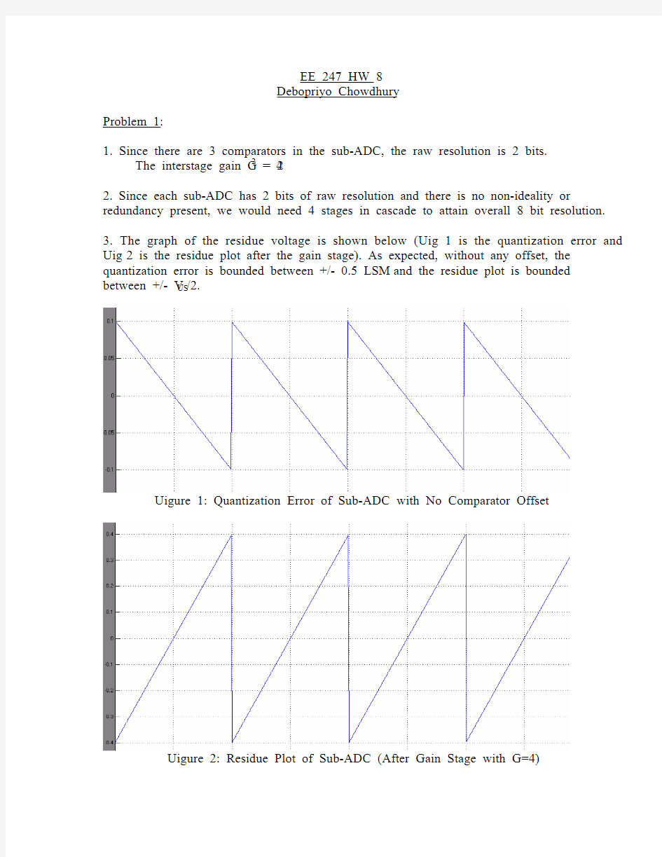
3. The graph of the residue voltage is shown below (Fig 1 is the quantization error and Fig 2 is the residue plot after the gain stage). As expected, without any offset, the quantization error is bounded between +/- 0.5 LSB and the residue plot is bounded between +/- V FS/2.
Figure 1: Quantization Error of Sub-ADC with No Comparator Offset
Figure 2: Residue Plot of Sub-ADC (After Gain Stage with G=4)
4. The offset voltages for the 3 comparators of the sub-ADC are 100mV, 0 and -100mV respectively. The quantization error is shown in Fig3 and the residue plot with gain of 4 is shown in Figure 4. As studied in lecture, because of comparator offset, the quantization error goes outside the bounds of +/- 0.5LSB and hence the residue goes out of the full scale range of the ADC.
Figure 3: Quantization Error of Sub-ADC with Comparator Offset
Figure 4: Residue Plot (After Gain Stage with G=4)
of Sub-ADC with Comparator Offset
5. From Figure 3, we see that due to offsets the quantization error is not bounded with +/- 0.5 LSB limits (+/- 100 mV) but instead varies between +/- 200mV. Hence to keep the residue after gain stage within full scale range, gain has to be reduced to 2.
The effective number of bits = log2G = 1
6. The first 3 stages have effective 1 bit each. The last stage does not feed any more sub-ADC after it and hence some overshoot might be tolerated by it. So it can have 2 bits. So net ADC number of bits = 5
Simulation Results:
The given setup was created in Simulink and the transfer characteristics were derived.
7. The transfer curve of the ADC (Vdigital vs Vanalog) is shown below.
Figure 5: Transfer Curve for the case when all stages are ideal
8. The transfer curve for the case when 1st ADC has offset is exactly same as Figure 5. The DNL and INL (calculated by doing a histogram test) are 0 LSB.
Figure 6: Histogram of Number of Points at each Code
As we can see that the number of points at all code are equal (the first and last are not considered in a histogram test) and hence DNL = 0 LSB. INL being cumulative sum of DNL is also 0.
Figure 7: INL and DNL when offset in only in first stage
9. The transfer curve when offset is in the last stage is also same as Figure 5. But this time, we have INL and DNL. Peak DNL = 0.47 LSB and peak INL = +/- 0.47 LSB.
Figure 8: Histogram
Figure 9: INL and DNL when offset in only in last stage
In all the 3 transfer curves, we see that for input signal ranging between –V FS/2 to + V FS/2, we have digital outputs from 8 to 39, indicating we have 32 levels. This agrees to our explanation that this is a 5 bit ADC. However, for inputs beyond this range, we still get digital outputs, as the curve shows, because truly we have 6 wires and the ADC can be a 5.5 bit one with input exceeding full scale range.
The difference in DNL/INL between the cases when offset is only in first stage versus when it is only in last stage can be explained as follows. The pipelined ADC designed has redundancy to accommodate any error that occurs due to comparator offset in first 3 stages. However, if it occurs in the last/4th stage, there is no one to take care of the overshoot in quantization error and hence we have worse DNL or INL performance.
As a side note, I saw that if the polarity of the offsets is reversed when the offset is only in the last stage, the ADC becomes non-monotonic as shown below.
Figure 10: Non-Monotonic Transfer Curve
Problem 2: Summary of Paper “ A 15b 1Ms/s Digitally Self-Calibrated Pipelined ADC” The primary accuracy limitations of a switched-capacitor pipelined ADC are capacitor mismatch, charge injection, finite operational amplifier gain and comparator offset. This paper proposes a completely digital self-calibration technique based on radix 1.93 that accounts for the non-idealities mentioned above. An important advantage of this design is that no extra analog circuitry, such as weighted capacitor arrays, and no extra clock cycles are required.
Unlike, analog calibration digital calibration alone does not correct or create analog decision levels. Therefore, the uncalibrated ADC must provide decision levels spaced no greater than 1 LSB at the intended resolution. This can be done by using redundancy in each stage and using lower gain to have smaller effective number of bits than raw number of bits for each sub-ADC.
The calibration algorithm for each stage is
Y=X, if D=0
Y= X+S1-S2+1, if D=1
Where Y is the calibrated code, X is the raw code and D is the bit decision.
Calibration starts from the last stage to be calibrated, namely the 11th stage. The 11th stage together with the following 6 uncalibrated stages is operated as a 7 bit ADC with 0V as input. From the resulting digital code, calibration constants S1 and S2 as shown in above equations, for the 11th stage are stored in memory. Next the calibration proceeds to 10th stage and in a similar manner upto the first stage.
The fully differential pipeline ADC is implemented in an 11V, 4 GHz, 2.4μm, BiCMOS process. The operational amplifier is a 2-stage design with a 100 MHz unity gain bandwidth and a 125 dB DC gain. The measured SDR is 88.1 dB, means their ENOB is about 14 bits. The DNL and INL performance of the calibrated ADC is also good. Problem 3:
Dynamic Range needed for 18 bit operation = 110.12 dB
a) No noise shaping, just pure oversampling
110.12/3 = 36.7 octave
Oversampling Ratio = 2^36.7 = 1.11 X 10^11
Sampling Frequency = 40k * 1.11 X 10^11 = 4.44 X 10^15 Hz
b) 1st order noise shaping
DR = -3.4 dB + 30 log (M)
M = 6081.35
Sampling frequency = 243.254 MHz
c) 2nd order noise shaping
DR = -11.1 dB + 50 log (M)
M= 265.7
Sampling frequency = 10.628 MHz
Option ? is better because it is a lower sampling frequency as compared to a second order sigma-delta modulator. Also, problems of limit cycle oscillation is less in second order sigma-delta modulators than in first-order.