AR0144 Streamlining Processor-based FPGA Design with the OpenBus System
Streamlining Processor-based FPGA Design with the OpenBus System
Summary
Article
AR0144 (v2.0) March 03, 2008 This document takes a look at Altium Designer's OpenBus System feature and how it can be used to simplify the creation of processor-based FPGA designs.
As the high-capacity, low-cost FPGA devices train continues its revolutionary journey through the electronics design landscape, an ever-increasing number of designers are jumping on board – trading their traditional hardware-based systems for the attractive lure of the FPGA's 'soft' programmability.
With Altium Designer, creation of soft processor-based systems, destined to run within a chosen target FPGA device, becomes second nature – utilizing one of the many supported flavors of 'soft' 32-bit RISC processor, wired up to access peripheral I/O and memory over a standard bus interface.
Like a prize chef creating his signature recipe, the designer builds his FPGA project choosing from an array of 'ingredient' building blocks – a 32-bit processor here, a pinch of peripheral I/O there and a dash of memory, all blended together using the appropriately configured Interconnect and Bus Mastering devices. Add to this the embedded software 'smarts' that will be running on the processor, and you have your 'icing on the cake' (or the pie filling from the processor's perspective!).
Up until now, such processor-based systems have typically been captured on a single schematic sheet. You may well have some descendent HDL entities, but each FPGA design project within Altium Designer must always have a single schematic top sheet. Such a design can rapidly become quite large and unwieldy – try fitting even the simplest of processor-based designs on a sheet size smaller than A3!
The design on the schematic also suffers from an inherent level of complexity, brought about by having to 'stitch' the bus interfaces of the various design components together. With a vast array of wiring, including additional clock and reset signals, mistakes can often creep in undetected until compilation.
To reduce the size and complexity of designs and, at the same time make creation of the design more intuitive and less prone to error, Altium Designer brings to the table its OpenBus System. The fundamental purpose of this system is to represent the processor, peripherals and related interconnections in a much more abstract way.
Wishbone Interface Background
The 32-bit processors and peripherals currently available for design in Altium Designer utilize the Wishbone bus standard. This standard is formally described as a "System-on-Chip Interconnection Architecture for Portable IP Cores". The current standard is the Revision B.3 Specification, a copy of which is included as part of the software installation and can be found by navigating to the Documentation Library ? Designing with FPGAs section of the Knowledge Center panel.
The Wishbone standard is not copyrighted and resides in the public domain. It may be freely copied and distributed by any means. Furthermore, it may be used for the design and production of integrated circuit components without royalties or other financial obligations. To this end, it is more commonly referred to as the Wishbone OpenBus standard.
The Wishbone standard is also implicitly device and vendor independent, making it very simple to create highly portable designs.
Wishbone OpenBus Processor Wrappers
To normalize access to hardware and peripherals, each of the 32-bit processors supported in Altium Designer has a Wishbone OpenBus-based FPGA core that 'wraps' around the processor. This enables peripherals defined in the FPGA to be used transparently with any type of processor. A Wishbone OpenBus wrapper around discrete, hard-wired peripherals also allows them to be moved seamlessly between processors.
The Wishbone OpenBus wrappers can be implemented in any FPGA and allow the designer to implement FPGA-based portable cores, taking advantage of the device driver system in Altium Designer for both FPGA-based soft-core peripherals as well as connections to off-chip discrete peripherals and memory devices.
Streamlining Processor-based FPGA Design with the OpenBus System
Processor Abstraction System
Use of Wishbone OpenBus wrappers creates a plug-in processor abstraction system that normalizes the interface to interrupt systems and other hardware specific elements. The system provides an identical interface to the processor's interrupt system, whether soft or hard-vectored. This allows different processors to be used transparently with identical source code bases.
Design Migration
With each 32-bit processor encased in a Wishbone OpenBus wrapper, an embedded software design can be seamlessly moved between soft-core processors, hybrid hard-core processors and discrete processors.
The Wishbone OpenBus wrapper makes each 32-bit processor architecturally similar, both in terms of memory map and pinout, giving a feeling of familiarity between processors and making the migration progress an intuitive and expedient one.
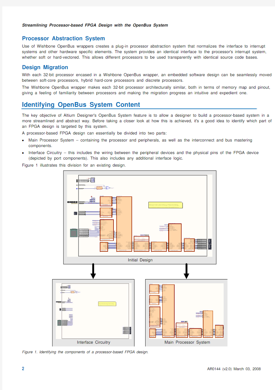
Identifying OpenBus System Content
The key objective of Altium Designer's OpenBus System feature is to allow a designer to build a processor-based system in a more streamlined and abstract way. Before taking a closer look at how this is achieved, it's a good idea to identify which part of an FPGA design is targeted by this system.
A processor-based FPGA design can essentially be divided into two parts:
?Main Processor System – containing the processor and peripherals, as well as the interconnect and bus mastering components.
?Interface Circuitry – this includes the wiring between the peripheral devices and the physical pins of the FPGA device (depicted by port components). This also includes any additional interface logic.
Figure 1 illustrates this division for an existing design.
Initial Design
Interface Circuitry Main Processor System
Figure 1. Identifying the components of a processor-based FPGA design.
Streamlining Processor-based FPGA Design with the OpenBus System
Altium Designer's OpenBus System feature is concerned purely with the representation of the main processor system within an FPGA design.
In an FPGA design that utilizes this system, the interface circuitry remains on
the schematic top-sheet – remember that all FPGA design projects in Altium
Designer must have a top-level schematic. The main processor system is
defined in a separate, OpenBus System document (*.OpenBus).
Connectivity between the two is made through a sheet symbol placed on the
schematic.
Figure 2. Example structure of an FPGA design
So how exactly does one go about building an OpenBus System in
using the OpenBus system.
AltiumDesigner? The whole process can be broken down into three key
stages:
?Place and wire the required devices that comprise the main processor system – this is then the OpenBus System. ?Configure the OpenBus System
?Connect the OpenBus System to the remaining interface circuitry of the FPGA design, resident on the top-level schematic sheet.
OpenBus System Design – Basics
At the heart of the OpenBus System is the OpenBus System document. This document is created and managed using Altium Designer's OpenBus Editor (Figure 3).
Figure 3. The OpenBus Editor.
The OpenBus Editor becomes active when the active document in the main design window is a *.OpenBus file. Create a new file of this type by right-clicking on the FPGA project entry in the Projects panel and choosing the Add New to Project ? OpenBus System Document command.
The OpenBus Editor has the familiar look and feel of Altium Designer's Schematic Editor, with a streamlined set of resources applicable to the creation of an OpenBus System. Filtering and inspection are provided courtesy of OpenBus Filter, OpenBus Inspector and OpenBus List panels, accessed from the OpenBus panel access button, to the bottom-right of the main design window.
The level of abstraction in place ensures that your processor-based design is created in a far more visual and intuitive way – think flow diagram on steroids and you would be pretty near the mark!
Streamlining Processor-based FPGA Design with the OpenBus System
System Building Blocks
The starting point for any OpenBus System document is the placement of
the required devices that will consitute your system. In the schematic world,
design components reside in libraries and are placed on the sheet directly
from the Libraries panel. In the OpenBus Editor, the corresponding
OpenBus components are placed from the OpenBus Palette panel (Figure
4).
The panel contains graphical representations of all devices available for use
in creating the system, grouped into the following five categories:
? Connectors – provides Interconnect and Arbiter components that are
functionally similar to the WB_INTERCON and WB_MULTIMASTER
devices in the schematic world. Additional components allow for bus
interface signals to be exposed outside of the OpenBus System
document. A termination port is also provided for occasions when a
master port is not being used and should be terminated properly.
? Processors – provides all of the 32-bit processors supported by Altium
Designer.
? Processor Wrappers – provides the discrete processors supported by
Altium Designer.
? Memories – provides memory controller devices.
? Peripherals – provides all of the I/O peripheral devices available for
design.
Should you wish to view more information about a particular component,
simply hover the cursor over its entry and a more detailed description will be
displayed in the lower region of the panel.
If the processor, peripheral and memory components are the 'bricks' of the
system, the Interconnect and Arbiter components can be thought of as the
'mortar' that brings them together. It is worth spending a moment to look at
the role of these two components, and why you would want to use them in
the first place.
The Role of the Interconnect Component
The Interconnect component provides a means of accessing one or more peripheral devices over a single OpenBus interface. It connects directly to
the IO or MEM ports of a processor component, facilitating communication with I/O peripherals or physical memory devices,
respectively. Figure 4. Place design primitives for your OpenBus
System from the OpenBus Palette panel.
For more information on the Interconnect component, refer to the TR0170 OpenBus Interconnect Component Reference . The Role of the Arbiter Component
The Arbiter component provides a simple means of sharing a slave peripheral device between multiple masters within the
OpenBus System. Typically, it is used where two or more devices require access to shared physical memory – for example two or more processors, or a processor and memory-based peripherals, such as a VGA Controller or a BT656 Video Capture
Controller.
For more information on the Arbiter component, refer to the TR0171 OpenBus Arbiter Component Reference .
Component Placement
Figure 5. Placement in a
couple of clicks.
Placement of OpenBus components is simply a case of clicking the required entry in the OpenBus
Palette panel, positioning at the desired location in the workspace, and clicking again to effect
placement. Familiar schematic placement controls, such as flipping and rotating allow for fine tuning
as needed.
Streamlining Processor-based FPGA Design with the OpenBus System Figure 6. Example designator.
Although each OpenBus component has a designator, it is not a designator in the schematic sense of the
word. There is no notion of annotation in the OpenBus System document. Rather, it is simply unique
comment text. This text will initially be the name of the component as used in the schematic world, along
with a suffix to distinguish multiple instances (e.g. WB_FPU_1). Change this text to a more meaningful
descriptor as required, but make sure the text of multiple instances of the same component are unique.
Bus Interface Ports
When an OpenBus component is placed, you will notice red and/or green circular appendages. These are
referred to as OpenBus ports and represent the bus interface(s) of the component:
-
a red port represents a master bus interface - a green port represents a slave bus interface A processor for example has two master ports, representing its Peripheral I/O and External Memory interfaces. The majority of peripherals have a single slave port. Some, like the VGA Controllers, have an additional master port, providing an interface to
external memory.
Figure 7. Example OpenBus components and their ports.
Wiring up the System
You've placed the required devices in your system, now it's time to
wire up those devices.
Figure 8. Component interfaces wired in a couple of clicks!
In the schematic world, wiring between devices requires individual
placement of wires and buses between corresponding pins of each
signal in the interface. In some cases, interconnect
(WB_INTERCON) and bus mastering (WB_MULTIMASTER)
devices might need to be graphically reconfigured so that pins of
interfaces line-up for nice parallel wiring. In other cases, the
position of interface pins may make full wiring less than desirable
and stub wiring with net labels is required.
In the OpenBus System, wiring is made very much simpler. The
individual bus interface signals are not exposed, only a single port
represents an interface. Two components are connected to each
other using a single link, referred to as an OpenBus link. Links are
made between ports of devices, with direction always being from a
master port (red) to a slave port (green).
Links can be added by clicking on the button on the OpenBus
toolbar (or by using the Place ? Link OpenBus Ports command).
A link is deleted simply by selecting it and pressing the Delete key.
When you enter link addition mode, all currently unlinked ports will
be filtered, with all other elements in the system dimmed.
If you click to start a link on a master port, all currently unlinked
slave ports will be filtered and available for choosing the
termination point of the link. Conversely, if you click to start a link
from a slave port, all currently unlinked master ports will be filtered
and made available.
Streamlining Processor-based FPGA Design with the OpenBus System
Note : You can start the link from either a master port or a slave port – the direction of the link itself will always be made to go from master to slave.
Rotate and/or flip OpenBus components in the system in order to facilitate easier linking of device ports and make the
description of the system more readable.
Graphical Editing
The following sections detail how components and links can be modified after placement within an OpenBus System.
Port Addition/Removal
When you initially place Interconnect and Arbiter components they will have a default number of
ports:
? Interconnect – one master port (m0) and one slave port (s0)
? Arbiter – one master port (m0) and two slave ports (s0 and s1).
It is highly likely that you will have more than one I/O peripheral in your design, and also
possible that more than two masters will need to share a memory resource. The
Interconnect and Arbiter components will therefore have to be modified to have the correct
number of ports.
Figure 9. Adding a port to an Interconnect component. To add a port, simply click on the button on the OpenBus toolbar (or use the Place ?
Add OpenBus Port command). A dimmed port shape will appear floating on the cursor.
As you move the shape next to the perimeter of a component, it will become solid – darker
gray with a blue outline (Figure 9). Position the new port as required and click to effect
placement.
Ports can also be clustered into groups around an Interconnect or Arbiter component. Up
to four cluster groups are possible (analogous to the four main points on a compass). To
add a new port to an existing group, ensure you place the port directly next to an existing
port in that group (Figure 10).
Figure 10. Clustering ports into groups.
To remove a port, simply click to select it in the workspace, then press the Delete key. The port will be removed from the component, providing such removal is valid. Interconnect and Arbiter components must always have at least one master and one slave port, which cannot be removed.
Note: Addition/removal of ports to/from all other component types is invalid and therefore will not be performed if attempted. Rearranging Ports
You may find, during the course of wiring up the OpenBus components, that certain ports could be better placed to ease wiring and make the system more readable. The OpenBus Editor provides the ability to change the location of a port (or ports) around a component.
To change the location of a port, simply click on the port and drag it to the required location on the perimeter of its parent component. Figure 11 illustrates this for a processor component, moving its IO and MEM interfaces ports to the left and right sides of the component respectively.
Streamlining Processor-based FPGA Design with the OpenBus System
Figure 11. Changing port location for an OpenBus component.
When rearranging ports around an Arbiter component, visible port numbers allow you to quickly identify each slave port. Arrange the ports and then wire up the master devices in the order of access required. Bear in mind that the physical location of a port has no bearing on the order in which the masters access the slave device(s), rather it is the port number to which each master device is linked.
Figure 12. Rearranging ports around an Arbiter component.
Reshaping Links
The shape of an OpenBus Link can be modified after placement – either manually, or by using one of the various link-related commands available on the OpenBus toolbar.
Manually Changing Link Shape
Clicking on an OpenBus Link after placement will display one or more editing handles for the link. Use these handles to graphically modify the shape of the link as required, to further enhance the readability of your OpenBus System.
Note: The end points of the link are not editable, only the shape of the link between. Once modified, the editor will attempt to keep the resulting shape, should the components connected by the link, or their applicable ports, be moved.
Streamlining Processor-based FPGA Design with the OpenBus System
Figure 13. Use editing handles to graphically modify the shape of a link after placement.
Automatically Normalizing Link Shape
If you have modified a link in any way, you can quickly revert back to its standard shape – the shape it had when first placed. To normalize a link, simply select it in the workspace and click on the button on the OpenBus toolbar. To normalize multiple links, simply ensure each link is included in the selection, prior to launching the command.
Figure 14. Normalizing a link.
Automatically Flipping Link Shape
Positions of components or other links may warrant the need to mirror, or flip the position of a link, to enhance readability of the system. To flip a link, simply select it in the workspace and click on the button on the OpenBus toolbar. To flip multiple links, simply ensure each link is included in the selection, prior to launching the command.
Figure 15. Flipping a link.
Streamlining Processor-based FPGA Design with the OpenBus System
Automatically Straightening Link Shape You may want to run a link directly from source master port to destination slave port with no curvature. Rather than adjusting positions of components to achieve a straight link, you can straighten the link itself. To straighten a link, simply select it in the
workspace and click on the button on the OpenBus toolbar. To straighten multiple links, simply ensure each link is included
in the selection, prior to launching the command.
Figure 16. Straightening a link. Configuring the OpenBus System
The key purpose of the OpenBus System feature is to facilitate creation of a
processor-based system as quickly, as intuitively and, perhaps more
importantly, as painlessly as possible. Building the actual system is a breeze,
but what about configuration? What steps are required to ensure correct
decoding widths, port data widths and addressing? Relax – configuring the
system just got a whole lot easier.
Figure 17. Access dialogs for configurable OpenBus components in the same way as their schematic-based counterparts.
In the schematic world, some components are configurable, for example
processors, certain peripherals, memory controllers and interconnects. The
corresponding representations of these components in the OpenBus world are
configured in a similar fashion – simply choose the Configure command from
the associated right-click menu, or double-click on the component directly.
Note: Double-clicking will bring up the main configuration dialog for the
component. If there are other configuration dialogs associated with the
component – typically applicable to processors only – these must be accessed
from the right-click menu.
Configuring Interconnect Components
Configuration of an Interconnect component is performed using the Configure
OpenBus Interconnect dialog (Figure 18). If you are familiar with configuration
of the WB_INTERCON component in the schematic world, you will no doubt
appreciate the reduced level of information required to configure the
Interconnect component. The OpenBus System handles much of the
configuration 'behind the scenes' as it were, so information such as data bus
width, addressing mode and device type no longer require user-definition. There is no manual addition/deletion of devices to/from the Interconnect. If a link exists between a peripheral and the
Interconnect, the device will automatically be listed
in the dialog.
Figure 18. Configuring an Interconnect component.
There is also no manual definition of the Master
Address Size. This too is taken care of in the
background, dependent on which port of the
processor the Interconnect is linked – IO (24-bit) or
MEM (32-bit).
There are, in fact, only three pieces of information
required to complete the configuration of the
Interconnect for each slave device – the Base
Address, the Decoder Address Width and the
Address Bus Size. Default information for each comes directly from the peripheral component itself.
For more information on configuring the Interconnect component, refer to the document TR0170 OpenBus Interconnect Component Reference
.
Streamlining Processor-based FPGA Design with the OpenBus System
Configuring Arbiter Components
Configuration of an Arbiter component is performed using the Configure
OpenBus Arbiter
dialog (Figure 19).
Figure 19. Configuring an Arbiter component. In comparison to its schematic counterpart – WB_MULTIMASTER –
configuration of the Arbiter is greatly streamlined. The OpenBus System once
again handles much of the configuration for you, so information such as data
and address bus widths no longer require user-definition.
Only two pieces of information are required through the dialog to configure the
Arbiter – the mode in which the masters access the shared slave(s), and which
master will be granted immediate access to the slave(s) when the Arbiter is in an
"Idle" state. These are the access Type and the Master With No Delay, respectively.
For more information on configuring the Arbiter component, refer to the document TR0171 OpenBus Arbiter Component Reference
.
Configuring Clock, Reset and Interrupt Lines
Management of the clock, reset and interrupt
lines for the system are handled in the
OpenBus Signal Manager dialog – accessed by clicking on the button on the OpenBus
toolbar (or using the Tools ? OpenBus
Signal Manager command). These signals
are handled separately from the bus
interface, leaving the interface to be just the
base set of standard bus signals.
Figure 20. Defining clock and reset lines for the OpenBus system.
Clock and reset signals across all
components in the system are listed over the
Clocks and Resets tabs of the dialog,
respectively (Figure 20). You can have all
clock/reset lines connected to a single,
default clock/reset net, such as CLK_I /
RST_I . Alternatively, you can specify a
particular net to which to connect to, on an
individual component basis.
Use of processor interrupt pins by slave
peripheral devices is determined on the
Interrupts
tab of the dialog (Figure 21).
Figure 21. Defining interrupt lines for the OpenBus system.
Streamlining Processor-based FPGA Design with the OpenBus System All interrupt-generating slave peripheral devices defined in the OpenBus System are listed, further
broken down into the individual interrupt lines they can provide. Each processor used in the system
will have a dedicated column. Use this column to specify which of the processor's interrupt pins, if
any, are to be used by the interrupt lines of each slave device.
Figure 22. Assigning a processor interrupt line to a slave peripheral device. Each interrupt line has an accompanying (and uneditable) graphical depiction of its Kind – whether
it is level-sensitive or edge-triggered – as well as its polarity.
Beneath the specific list of defined OpenBus peripherals and their interrupts, there is a complete
listing of all interrupt pins for the processor, allowing the ability to export interrupt lines.
If an interrupt line is not currently assigned to an OpenBus peripheral, it can be made available as an input pin on the top-level design schematic. This enables you to import an interrupt from a peripheral device external to the OpenBus System document. Simply use the associated drop-down field and set the entry to Exported (as input pin)
.
Figure 23. Exporting a processor interrupt line for use as input by an external peripheral device.
The Kind and Polarity field will become editable, from where you can specify the type of interrupt being imported on this line
(Figure 24).
Figure 24. Setting interrupt kind for the external interrupt.
If an interrupt line is currently assigned to an OpenBus peripheral, it can be made available as an output pin on the top-level design schematic. This enables you, for example, to export an interrupt for debugging purposes, or for connection to a processor that resides on the schematic sheet. Simply set the entry in the associated field for the interrupt to Exported (as output pin). Figure 25 illustrates this for a series of processor interrupt pins assigned for use by internal OpenBus peripheral
devices.
Figure 25. Exporting processor interrupt lines for use outside of the OpenBus System.
Note: An exported interrupt will change from being an input pin to an output pin, if that interrupt becomes assigned to an OpenBus peripheral component. If the interrupt is no longer connected to the OpenBus peripheral, the exported interrupt will
Streamlining Processor-based FPGA Design with the OpenBus System
change from output pin to input pin. In all cases, resynchronization between the sheet entries on the top sheet and the ports of the OpenBus System document must be performed.
For interrupt pin INT_I0, there is an additional entry that can be chosen – Internal. This allows for the situation where the INT_I0 line of the processor is actually the logical OR of the interrupt generated by a Programmable Interval Timer, internal to the processor, and the interrupt line zero. Provided the interrupt is not assigned to an OpenBus peripheral, the Internal entry will be available. When this option is used, the interrupt pin will not be exported for use outside the OpenBus System. Note however, that precedence is given to use of the interrupt line by an OpenBus peripheral. If you have set the Internal option for the pin, then subsequently assign INT_I0 for a peripheral's interrupt line, the setting will automatically be changed to Exported (as output pin).
For an example of exporting interrupt lines, see the section Handling External Interrupts, later in this document. Configuring Processor Memory and Peripherals
An OpenBus System incorporating a 32-bit processor will typically involve the connection of slave memory and peripheral devices – to the processor's MEM and IO ports respectively. Unlike schematic-based design however, you are not required to manually define the mapping of these devices into the processor's address space, it is handled for you. The mapping information is supplied through the respective configuration dialogs (processor, peripherals, memories and interconnects). The OpenBus System simply takes this information and dynamically maps each device memory or peripheral device accordingly.
The resulting 'memory map', as it is often called, is essentially the bridge between the hardware and software projects – the hardware team allocating each of the various memory and peripheral devices their own chunk of the processor's address space, the software team then writing their code to access the memory and peripherals at given locations.
Mapping Overview
Processor address space can be configured from within the OpenBus System (both memory and peripheral I/O) or the Embedded Software project (memory only). In terms of memory, there are two key pieces of terminology to be aware of:
?Device Memory – these are blocks of memory that are mapped into the processor's memory architecture (i.e. its address space) based on the physical memory defined in the system. From the OpenBus System document, this is handled
automatically (and dynamically). From the Embedded Software project, this can be achieved by manually importing directly from the FPGA project, or by automatically importing from the FPGA project upon compilation.
?Application Memory – these are defined blocks of memory corresponding to the mapped blocks of device memory.
Definable from the Embedded Software project only, these blocks enable you to handcraft exactly how the device memory is used by the embedded code. By default, an application memory block will be the same definition as its 'parent' device memory block. You might decide to define the application memory block to be smaller in size or maybe define multiple sub-blocks within the available application memory block.
Note: Device memory can not be manually defined or edited through the respective memory configuration dialogs. Such memory can only be changed by changing the configuration of the physical memory device itself.
You can also generate .asm and/or .h files for the Embedded Software project, upon FPGA project compilation, providing a means to quickly and efficiently address devices from within the embedded source code.
Figure 26 summarizes the key elements to defining processor address space in terms of memory and peripheral I/O and where such elements can be defined.
Streamlining Processor-based FPGA Design with the OpenBus System OpenBus System Document (*.OpenBus)
Automatically and dynamically
updated
Figure 26. Key elements used to define processor address space.
Verification of Mapping from within the OpenBus System
Within the OpenBus System, defined memories and peripheral I/O devices will be automatically mapped into the processor's address space.
From within the OpenBus System, this mapping can be verified using the Configure Processor Memory and Configure Peripherals dialogs, respectively (Figure 27). Access these dialogs by right-clicking on the graphical representation of the processor and choosing Configure Processor Memory or Configure Processor Peripheral from the context menu that appears. The mapping is dynamic – any changes made to physical memory devices or peripheral I/O (e.g. base addresses) will be reflected directly in these dialogs.
Should you wish to generate the corresponding assembly or C header file for the hardware in the system, ensure that the respective option to generate hardware.asm (Assembly File) or hardware.h (C Header File) is enabled. Enabling an option in one dialog will automatically enable it in the other. When you compile the FPGA project again, the respective file(s) will be generated and added as source to the linked Embedded Software project.
Streamlining Processor-based FPGA Design with the OpenBus System
Figure 27. Verifying configuration of processor memory and peripheral I/O from within the OpenBus system.
Streamlining Processor-based FPGA Design with the OpenBus System Interfacing to the Schematic Sheet
With the OpenBus System defined and configured, the system now needs to be interfaced with the top-level schematic in the FPGA design. This, as has been mentioned previously, is handled through a sheet symbol placed on the schematic sheet.
The sheet entries required to populate the sheet symbol can be obtained through use of the sheet entries and ports synchronization feature. Access this feature through the Sheet Symbol Actions ? Synchronize Sheet Entries and Ports command, available from the right-click context menu for the sheet symbol. The Synchronize Ports To Sheet Entries On System dialog will appear (Figure 28).
Figure 28. Use the synchronize sheet entries and ports feature to hook-up the OpenBus System.
All ports from the OpenBus System document will be initially listed as unmatched ports. The ports themselves actually come from three places:
?Ports automatically derived based on the external interfaces of the peripheral devices (I/O peripherals and memory controllers). These ports are summarized on the External connection summary tab of the OpenBus Signal Manager dialog.
?Ports derived from the clock and reset line net definitions on the Clocks and Resets tabs of the OpenBus Signal Manager dialog.
Streamlining Processor-based FPGA Design with the OpenBus System
?Ports derived from exported interrupt line definitions on the Interrupts tab of the OpenBus Signal Manager dialog.
When using the dialog to add sheet entries to the sheet symbol, it is a good idea to select each bank of related ports in turn, rather than all ports at once. This will make placement of the sheet entries within the sheet symbol that much easier. Simply group select the required ports and click the Add Sheet Entries button beneath the list – the sheet entries will float on the cursor ready for placement (Figure 29).
Figure 29. Sheet entry placement.
Once sheet entries for all ports have been added, the sheet symbol will be fully synchronized with the underlying OpenBus System.
Note: You can of course use the Create Sheet Symbol From Sheet Or HDL command (accessed from the Design menu in the schematic) to generate the sheet symbol quickly and in a more automated way. However, if used after the OpenBus System is defined, all sheet entries will be placed at once with no control.
Mopping up – Interface Circuitry
The last stage required to fully hook the OpenBus System into the FPGA design is to wire-up the interface circuitry on the top-level schematic. This circuitry includes the wiring between devices in the OpenBus System and the physical pins of the FPGA device. Any additional logic devices will also reside on this top-sheet. Remember that the extents of the OpenBus System are the sheet entries of the sheet symbol on the top-level schematic. The representation of the physical pins of the FPGA device are the port components that are placed on the schematic. The job becomes a simple one – wire between the two.
Note: You may need to rearrange sheet entries for peripheral interfaces, in order to match the layout of the port components and thereby make the schematic wiring as neat and as readable as possible.
Figure 30 illustrates an example of this interface circuitry, wired up to the sheet symbol. Notice also that the required components for implementation of the Soft JTAG chain – the NEXUS_JTAG_CONNECTOR and NEXUS_JTAG_PORT – are also included on the sheet. Figure 31 shows the underlying OpenBus System for this design, which is referenced by the sheet symbol.
Streamlining Processor-based FPGA Design with the OpenBus System
Figure 30. Wired interface circuitry.
Figure 31. Example underlying OpenBus System, referenced by the sheet symbol on the top-level schematic.
Streamlining Processor-based FPGA Design with the OpenBus System
Accommodating Schematic-based Devices
Building the main processor system solely within the self-contained walls of the OpenBus System document will be an attractive solution for the majority of designs. However, you may need (or even want) to separate certain devices from the system, and have them reside on the top-level schematic sheet. For example, you may be using additional components that are not supported as graphical representations in the OpenBus Palette panel, and therefore cannot be placed within the OpenBus System document. Not a problem.
Two connector components are available from the OpenBus Palette panel that facilitate the use of external, schematic-based devices, within the overall processor-based system:
- Bus Importer component. This component exposes bus interface signals external to the OpenBus System document. It allows you to wire from the master interface of a device on the schematic sheet to a
slave port of a component in the OpenBus System.
- Bus Exporter component. This component exposes bus interface signals external to the OpenBus System document. It allows you to wire from the master port of a component in the OpenBus System to
the slave interface of a device on the schematic sheet.
There's nothing like an example to better illustrate a concept and hit home the power of a feature. To give you an idea of how these Bus Importer and Exporter components are used in a design, let us consider the FPGA design and constituent OpenBus System of figures 30 and 31 in the previous section. To keep this example simple, we will just add a couple of devices to the top-level schematic – a MicroBlaze 32-bit RISC processor and an Infrared Decoder (Figure 32).
Figure 32. Additional devices on the schematic sheet.
In this example, the processor will share access to the bank of peripherals currently accessed by the TSK30000A. The Infrared Decoder will be an addition to this group, resulting in the two processors sharing access to the following five peripheral devices:
?Floating Point Unit
?Parallel Port Unit
? SPI Controller
?VGA Controller with TFT Interface
? Infrared Decoder.
Streamlining Processor-based FPGA Design with the OpenBus System The first step is to modify the OpenBus System document, with use of Bus Importer and Exporter components to provide links to
the external processor and Infrared Decoder devices respectively (Figure 33).
Figure 33. Modifying the OpenBus System with inclusion of Bus Importer and Exporter connectors.
Notice also, the use of a second Arbiter component in
the system, to allow the two processors to share the
peripherals.
Figure 34. Configuring Bus Importer and Exporter components.
Prior to returning to the schematic sheet to finalize the
wiring, there are some additional configuration steps
to be performed from the OpenBus System document.
Firstly, the Bus Importer and Exporter components
must be configured in relation to the external
interfaces they are connecting to. This involves setting
the Address Mode, Address and Data bus widths, as
well as specifying that data and select lines are to be
made available outside of the OpenBus System
document (Figure 34).
Next, the base address for the Infrared Decoder
peripheral must be defined, in the configuration dialog
for the associated Interconnect component (Figure 35). The initial information comes directly from the
configured Bus Exporter component.
Figure 35. Specifying base address for the new schematic-based peripheral.
Streamlining Processor-based FPGA Design with the OpenBus System
The new peripheral is automatically mapped into the TSK3000A processor's address space (Figure 36).
Figure 36. Mapping of new schematic-based peripheral into processor address space.
Once the wiring and configuration is
finalized in the OpenBus System
document, you can then turn your
attention back to the schematic top-
sheet.
Figure 37. Wiring the schematic-based devices 'into' the OpenBus System. Use the Synchronize Sheet Entries
and Ports feature for the sheet
symbol, and place the additional
sheet entries relating to the Bus
Importer and Exporter components.
Rearrange sheet entries within each
interface as necessary and then wire
each interface signal to its
corresponding pin of the processor
and Infrared Decoder devices (Figure
37).
Once the wiring is in place, the
processor in the OpenBus System
has access to the Infrared Decoder
device. Likewise, the processor on the
schematic can access both the
peripheral on the sheet, as well as all
peripheral devices defined in the
underlying OpenBus System.
Remember to map the peripherals into the schematic processor's
memory.