HDSP-A511-JK000中文资料
Devices AlGaAs Orange Red HER Green Package HDSP-HDSP-HDSP-HDSP-Description
Drawing A411A111A211A5117.6 mm Common Anode Right Hand Decimal A A413A113A213A5137.6 mm Common Cathode Right Hand Decimal B F411F111F211F51110 mm Common Anode Right Hand Decimal C F413F113F213F51310 mm Common Cathode Right Hand Decimal D G411G111G211G51110 mm Two Digit Common Anode Right Hand Decimal E G413G113G213G51310 mm Two Digit Common Cathode Right Hand Decimal F H411H111H211H51114.2 mm Common Anode Right Hand Decimal G H413H113H213H51314.2 mm Common Cathode Right Hand Decimal H K411K111K211K51114.2 mm Two Digit Common Anode Right Hand Decimal I K413
K113
K213
K513
14.2 mm Two Digit Common Cathode Right Hand Decimal
J
Description
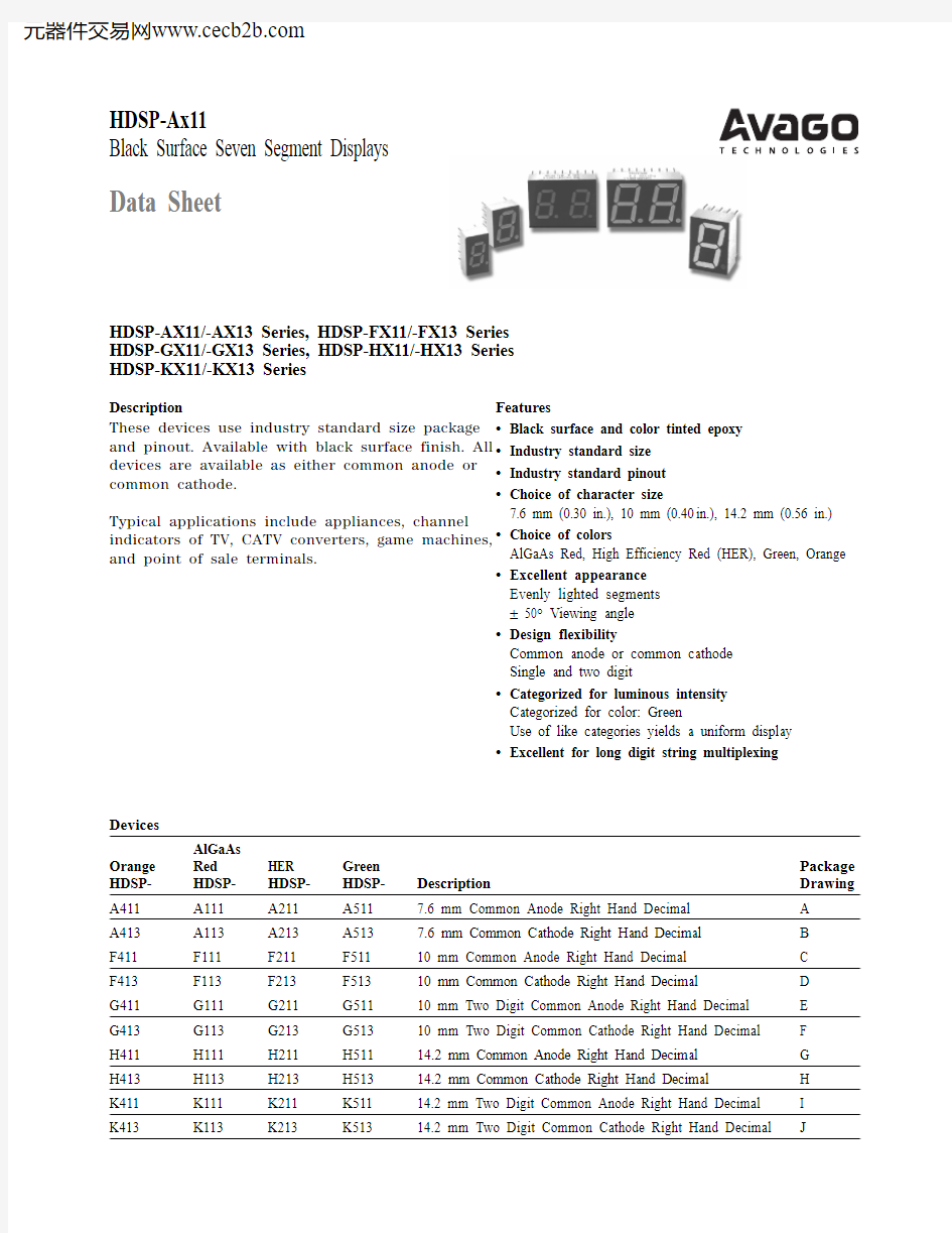
These devices use industry standard size package and pinout. Available with black surface finish. All devices are available as either common anode or common cathode.
Typical applications include appliances, channel indicators of TV, CATV converters, game machines,and point of sale terminals.
HDSP-AX11/-AX13 Series, HDSP-FX11/-FX13 Series HDSP-GX11/-GX13 Series, HDSP-HX11/-HX13 Series HDSP-KX11/-KX13 Series
Features
?Black surface and color tinted epoxy ?Industry standard size ?Industry standard pinout ?Choice of character size
7.6 mm (0.30 in.), 10 mm (0.40in.), 14.2 mm (0.56 in.)?Choice of colors
AlGaAs Red, High Efficiency Red (HER), Green, Orange ?Excellent appearance Evenly lighted segments ± 50° Viewing angle ?Design flexibility
Common anode or common cathode Single and two digit
?Categorized for luminous intensity Categorized for color: Green
Use of like categories yields a uniform display ?
Excellent for long digit string multiplexing
HDSP-Ax11
Black Surface Seven Segment Displays
Data Sheet
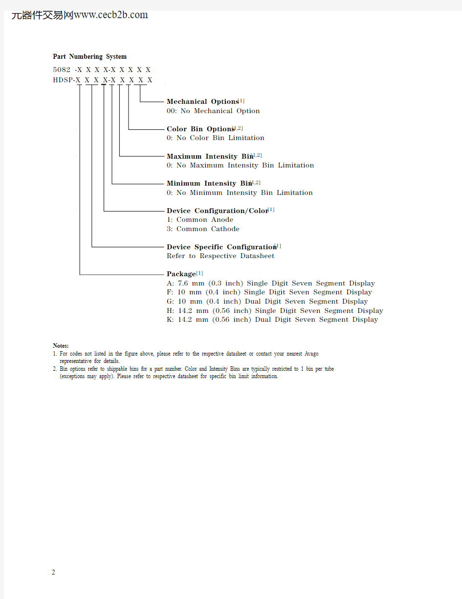
Part Numbering System
5082 -X X X X-X X X X X
HDSP-X X X X-X X X X X
Mechanical Options[1]
00: No Mechanical Option
Color Bin Options[1,2]
0: No Color Bin Limitation
Maximum Intensity Bin[1,2]
0: No Maximum Intensity Bin Limitation
Minimum Intensity Bin[1,2]
0: No Minimum Intensity Bin Limitation
Device Configuration/Color[1]
1: Common Anode
3: Common Cathode
Device Specific Configuration[1]
Refer to Respective Datasheet
Package[1]
A: 7.6 mm (0.3 inch) Single Digit Seven Segment Display
F: 10 mm (0.4 inch) Single Digit Seven Segment Display
G: 10 mm (0.4 inch) Dual Digit Seven Segment Display
H: 14.2 mm (0.56 inch) Single Digit Seven Segment Display
K: 14.2 mm (0.56 inch) Dual Digit Seven Segment Display Notes:
1.For codes not listed in the figure above, please refer to the respective datasheet or contact your nearest Avago
representative for details.
2.Bin options refer to shippable bins for a part number. Color and Intensity Bins are typically restricted to 1 bin per tube
(exceptions may apply). Please refer to respective datasheet for specific bin limit information.
Package Dimensions (7.6 mm Series)Internal Circuit Diagram
Package Dimensions (10 mm Series: Single)Internal Circuit Diagram
Package Dimensions (14.2 mm Series: Two Digit)Internal Circuit Diagram
2
1DIGIT NO. 1 CATHODE
Absolute Maximum Ratings
AlGaAs Red HER/Orange Green
HDSP-X11X HDSP-X21X/X41X HDSP-X51X Description Series Series Series Units Average Power per Segment or DP37105105mW Peak Forward Current per Segment or DP4590[1]90[3]mA DC Forward Current per Segment or DP15[5]30[2]30[4]mA Operating Temperature Range–20 to +100 –40 to +100°C Storage Temperature Range–55 to +100°C Reverse Voltage per Segment or DP 3.0V Wave Soldering Temperature for 3 Seconds250°C (1.60 mm [0.063 in.] below Body)
Notes:
1. See Figure 5 to establish pulsed conditions.
2. Derate above 53°C at 0.45 mA/°C (see Figure 7).
3. See Figure 6 to establish pulsed conditions.
4. Derate above 39°C at 0.37 mA/°C (see Figure 7).
5. Derate above 91°C at 0.53 mA/°C (see Figure 1).
Electrical/Optical Characteristics at T A = 25°C
AlGaAs Red
Device Series
HDSP-Parameter Symbol Min.Typ.Max.Units Test Conditions A11X Luminous Intensity/Segment[1,2]I V315600μcd I F = 1 mA (Digit Average)3600I
F = 5 mA
F11X, G11X330650I F = 1 mA
3900I F = 5 mA
H11X, K11X400700I F = 1 mA
4200I F = 5 mA
All Devices Forward Voltage/Segment or DP V F 1.6 2.0V I F = 1 mA
1.7I F = 5 mA
1.822I F = 20 mA Peak
Peak Wavelength l PEAK645nm
Dominant Wavelength[3]l d637nm
Reverse Voltage/Segment or DP[4]V R 3.015V I R = 100 μA
Temperature Coefficient of?V F/°C-2mV/°C
V F/Segment or DP
A11X Thermal Resistance LED R q J-PIN255°C/W/
F11X, G11X Junction-to-Pin
320
Seg.
H11X, K12X400
High Efficiency Red Device Series HDSP-Parameter
Symbol Min.Typ.Max.
Units Test Conditions A21X Luminous Intensity/Segment [1,2]I V
360980μcd
I F = 5 mA (Digit Average)
5390I F = 20 mA F21X, G21X 4201200I F = 5 mA H21X, K21X
900
2800I F = 10 mA 3700
I F = 60 mA Peak:1/6 Duty Factor All
Forward Voltage/Segment or DP V F 2.0 2.5
V I F = 20 mA
Devices
Peak Wavelength l PEAK 635nm Dominant Wavelength [3]
l d 626nm Reverse Voltage/Segment or DP [4]V R 3.0
30V I R = 100 μA
Temperature Coefficient of ?V F /°C -2mV/°C V F /Segment or DP
A21X Thermal Resistance LED R q J-PIN
200°C/W/F21X, G21X Junction-to-Pin
320Seg.
H21X, K21X
345
Orange Device Series HDSP-Parameter
Symbol Min.
Typ.Max.
Units Test Conditions A41X Luminous Intensity/Segment I V
0.70mcd
I F = 5 mA F41X, G41X (Segment Average)[1,2]
1.0I F = 5 mA H41X, K41X
2.37I F = 10 mA All
Forward Voltage/Segment or DP V F 2.0 2.5
V I F = 20 mA
Devices
Peak Wavelength l PEAK 600nm Dominant Wavelength [3]
l d 603nm Reverse Voltage/Segment or DP [4]V R 3.0
30V I R = 100 μA
Temperature Coefficient of ?V F /°C –2mV/°C V F /Segment or DP
A41X Thermal Resistance LED R q J-PIN
200°C/W/F41X, G41X Junction-to-Pin
320Seg.
H41X, K41X
345
High Performance Green
Device Series
HDSP-Parameter Symbol Min.Typ.Max.Units Test Conditions
A51X Luminous Intensity/Segment[1,2]I V8603000μcd I F = 10 mA (Digit Average)6800I
F = 20 mA
F51X, G51X10303500I F = 10 mA
H51X, K51X9002500I F = 10 mA
3100I F = 60 mA Peak:
1/6 Duty Factor All Forward Voltage/Segment or DP V F 2.1 2.5V I F = 10 mA
Devices Peak Wavelength l
PEAK566nm
Dominant Wavelength[3,5]l d571577nm
Reverse Voltage/Segment or DP[4]V R 3.050V I R = 100 μA
Temperature Coefficient of?V F/°C-2mV/°C
V F/Segment or DP
A51X Thermal Resistance LED R q J-PIN200°C/W/
F51X, G51X Junction-to-Pin320Seg.
H51X, K51X345
Notes:
1. Case temperature of device immediately prior to the intensity measurement is 25°C.
2. The digits are categorized for luminous intensity. The intensity category is designated by a letter on the side of the package.
3. The dominant wavelength, l d, is derived from the CIE chromaticity diagram and is that single wavelength which defines the color of the device.
4. Typical specification for reference only. Do not exceed absolute maximum ratings.
5. Green (HDSP-A51X/F51X/G51X/H512X/K51X) series displays are categorized for dominant wavelength. The category is designated by a number
adjacent to the luminous intensity category letter.
Figure 3. Relative luminous intensity vs. dc forward current.
current) vs. peak current.
Figure 1. Maximum allowable average or dc
current vs. ambient temperature.
Figure 2. Forward current vs. forward voltage.
F 50.020.0
10.05.02.01.00.50.1
0.5
1.0
1.5
2.0
2.5
V – FORWARD VOLTAGE – V F
I – F O R W A R D C U R R E N T
P E R S E G M E N T – m A
20
105
210.5
0.20.10.1
0.2
0.5
1
2
5
10
20
R E L A T I V E L U M I N O U S I N T E N S I T Y (N O R M A L I Z E D T O 1 A T 1 m A )
I – FORWARD CURRENT PER SEGMENT – mA
F
AlGaAs Red
HER, Green, Orange
Figure 7. Maximum allowable dc current vs.
ambient temperature.Figure 8. Forward current vs. forward voltage characteristics.
Figure 9. Relative luminous intensity vs. dc forward current.Figure 10. Relative efficiency (luminous intensity per unit current) vs. peak current.
400510152025303520
1009080
7060
50
40
30T – AMBIENT TEMPERATURE – °C A
I M A X – M A X I M U M D C C U R R E N T P E R S E G M E N T – m A
D C 120
11050
45
0100
80
60
40
20
I – F O R W A R D C U R R E N T P E R S E G M E N T – m A
F
V – FORWARD VOLTAGE – V F
ηP E A K – R E L A T I V E L U M I N O U S I N T E N S I T Y (N O R M A L I Z E D T O 1 A T 5 m A F O R H E R , A N D T O 1 A T 10 m A F O R G R E E N )
150
10
8
6
4
220530
1025I – FORWARD CURRENT PER SEGMENT – mA F
I – PEAK FORWARD CURRENT PER SEGMENT – mA
PEAK
ηP E A K – R E L A T I V E E F F I C I E N C Y (N O R M A L I Z E D T O 1 A T 5 m A F O R H E R , A N D 10 m A F O R G R E E N )
Figure 5. Maximum tolerable peak current vs. pulse
duration – HER, Orange.Figure 6. Maximum tolerable peak current vs.pulse duration – Green.
Intensity Bin Limits (mcd) AlGaAs Red Orange
HDSP-A41X
IV Bin Category Min Max A0.2840.433 B0.3540.541 C0.4430.677 D0.5540.846 E0.692 1.057 F0.856 1.322
G 1.082 1.652
H 1.352 2.066
I 1.692 2.581 J 2.114 3.227 K 2.641 4.034 L 3.300 5.042 M 4.127 6.303 N 5.1577.878
HDSP-F41X/G41X
IV Bin Category Min Max C0.4850.890 D0.728 1.333
E 1.091 2.000
F 1.636 3.000
G 2.454 4.500
H 3.682 6.751
HDSP-H41X/K41X
IV Bin Category Min Max B0.77 1.17 C0.95 1.45
D 1.19 1.82
E 1.49 2.27
F 1.85 2.89
G 2.32 3.54
H 2.90 4.43
HDSP-A1xx
IV Bin Category Min.Max. E0.3150.520 F0.4280.759 G0.621 1.16 H0.945 1.71 I 1.40 2.56 J 2.10 3.84 K 3.14 5.75 L 4.708.55
HDSP-F1xx/G1xx
IV Bin Category Min.Max. D0.3910.650 E0.5320.923 F0.755 1.39
G 1.13 2.08
H 1.70 3.14
HDSP-H1xx/K1xx
IV Bin Category Min.Max. C0.4150.690 D0.5650.990 E0.810 1.50
F 1.20 2.20
G 1.80 3.30
H 2.73 5.00
I 4.097.50
Intensity Bin Limits (mcd), continued HER
HDSP-A2xx
IV Bin Category Min.Max. B0.3420.630 C0.5160.946 D0.774 1.418
E 1.160 2.127
F 1.740 3.190
G 2.610 4.785
H 3.9157.177
HDSP-F2xx/G2xx
IV Bin Category Min.Max. C0.4850.890 D0.728 1.333
E 1.091 2.000
F 1.636 3.000
G 2.454 4.500
H 3.682 6.751
HDSP-H2xx/K2xx
IV Bin Category Min.Max. E0.91 1.67
F 1.37 2.51
G 2.05 3.76
H 3.08 5.64
I 4.628.64 J 6.9312.70 K10.3919.04
Contrast Enhancement
For information on contrast enhancement, please see Application Note 1015.Soldering/Cleaning
For information on soldering LEDs, please refer to Application Note 1029.
Electrical/Optical
For more information on
electrical/optical characteristics,please see Application Note 1005.
Note:
All categories are established for classification of products. Products may not be available in all categories. Please contact your Avago representatives for further clarification/information.
HDSP-A5xx IV Bin Category Min.Max.H 0.86 1.58I 1.29 2.37J 1.94 3.55K 2.90 5.33L
4.37
8.01
HDSP-F5xx/G5xx IV Bin Category Min.Max.H 1.54 2.82I 2.31 4.23J 3.46 6.34K 5.189.50L
7.78
14.26
HDSP-H5xx/K5xx IV Bin Category Min.Max.E 0.91 1.67F 1.37 2.51G 2.05 3.76H 3.08 5.64I
4.61
8.46
Intensity Bin Limits (mcd), continued Green
Color Categories
Dominant Wavelength (nm)
Color Bin Min.Max.Green
2573.00577.003570.00574.004567.00571.005
564.00
568.00
For product information and a complete list of distributors, please go to our website: https://www.wendangku.net/doc/e318271999.html, Avago, Avago Technologies, and the A logo are trademarks of Avago Technologies, Pte. in the United States and other countries. Data subject to change. Copyright ? 2006 Avago Technologies Pte. All rights reserved. Obsoletes 5988-4433EN
5989-2795EN April 10, 2006