A25L080

8Mbit / 4Mbit Low Voltage, Serial Flash Memory
With 100MHz Uniform 4KB Sectors
Document Title
8Mbit / 4Mbit, Low Voltage,Serial Flash Memory With 100MHz Uniform 4KB Sectors
Revision History
Date Remark Rev. No. History Issue
0.0 Initial issue July 9, 2007 Preliminary
1.0 Add the maximum clock rate of 3.0V~3.6V : 100MHz October 8, 2007 Final
Final version release
8Mbit / 4Mbit Low Voltage, Serial Flash Memory
With 100MHz Uniform 4KB Sectors
FEATURES
Family of Serial Flash Memories
- A25L080: 8M-bit /1M-byte
- A25L040: 4M-bit /512K-byte
Flexible Sector Architecture with 4KB sectors - Sector Erase (4K-bytes) in 0.4s (typical)
- Block Erase (64K-bytes) in 1s (typical)
Page Program (up to 256 Bytes) in 3ms (typical) 2.7 to 3.6V Single Supply Voltage
SPI Bus Compatible Serial Interface
100MHz Clock Rate (maximum)
Deep Power-down Mode 1μA (typical) Electronic Signatures
- JEDEC Standard Two-Byte Signature
A25L080: (3014h)
A25L040: (3013h)
- RES Instruction, One-Byte, Signature, for backward compatibility
A25L080 (13h)
A25L040 (12h)
Package options
-8-pin SOP (150/209mil), 8-pin DIP (300mil)
- All Pb-free (Lead-free) products are RoHS compliant
GENERAL DESCRIPTION
The A25L080/A25L040 are 8M/4M bit Serial Flash Memory, with advanced write protection mechanisms, accessed by a high speed SPI-compatible bus.
The memory can be programmed 1 to 256 bytes at a time, using the Page Program instruction.
The memory is organized as 16/8(A25L080/A25L040) blocks, each containing 16 sectors. Each sector is composed of 16 pages. Each page is 256 bytes wide. Thus, the whole memory can be viewed as consisting of 4096/2048(A25L080/A25L040) pages, or 1048,576/524,288(A25L080/A25L040) bytes.
The whole memory can be erased using the Chip Erase instruction, a block at a time, using Block Erase instruction, or a sector at a time, using the Sector Erase instruction.
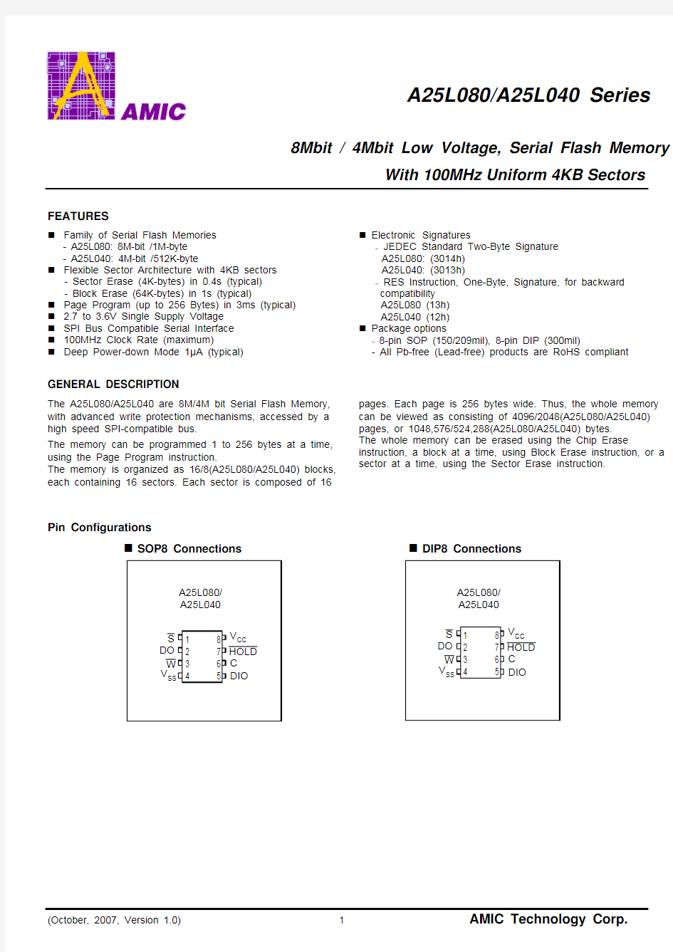
Pin Configurations
SOP8 Connections DIP8 Connections
Block Diagram
C HOLD
W
S
Pin Descriptions
1. The DIO is also used as an output pin when the Fast Read Dual Output instruction and the Fast Read Dual Input-Output instruction are executed.
2. The DO is also used as an input pin when the Fast Read Dual Input-Output instruction is executed.
Logic Symbol
SS
V
SIGNAL DESCRIPTION
Serial Data Output (DO). This output signal is used to transfer data serially out of the device. Data is shifted out on the falling edge of Serial Clock (C).
The DO pin is also used as an input pin when the Fast Read Dual Input-Output instruction is executed.
Serial Data Input (DIO). This input signal is used to transfer data serially into the device. It receives instructions, addresses, and the data to be programmed. Values are latched on the rising edge of Serial Clock (C).
The DIO pin is also used as an output pin when the Fast Read Dual Output instruction and the Fast Read Dual Input-Output instruction are executed.
Serial Clock (C). This input signal provides the timing of the serial interface. Instructions, addresses, or data present at Serial Data Input (DIO) are latched on the rising edge of Serial Clock (C). Data on Serial Data Output (DO) changes after the falling edge of Serial Clock (C).
Chip Select (S). When this input signal is High, the device is deselected and Serial Data Output (DO) is at high impedance. Unless an internal Program, Erase or Write Status Register cycle is in progress, the device will be in the Standby mode (this is not the Deep Power-down mode). Driving Chip Select (S) Low enables the device, placing it in the active power mode.
After Power-up, a falling edge on Chip Select (S) is required prior to the start of any instruction.
Hold (HOLD). The Hold (HOLD) signal is used to pause any serial communications with the device without deselecting the device.
During the Hold condition, the Serial Data Output (DO) is high impedance, and Serial Data Input (DIO) and Serial Clock (C) are Don’t Care. To start the Hold condition, the device must be selected, with Chip Select (S) driven Low. Write Protect (W). The main purpose of this input signal is to freeze the size of the area of memory that is protected against program or erase instructions (as specified by the values in the BP2, BP1, and BP0 bits of the Status Register).
SPI MODES
These devices can be driven by a microcontroller with its SPI peripheral running in either of the two following modes: – CPOL=0, CPHA=0 – CPOL=1, CPHA=1
For these two modes, input data is latched in on the rising edge of Serial Clock (C), and output data is available from the
falling edge of Serial Clock (C).
The difference between the two modes, as shown in Figure 2, is the clock polarity when the bus master is in Stand-by mode and not transferring data:
– C remains at 0 for (CPOL=0, CPHA=0) – C remains at 1 for (CPOL=1, CPHA=1)
Figure 1. Bus Master and Memory Devices on the SPI Bus
Note: The Write Protect (W ) and Hold (HOLD ) signals should be driven, High or Low as appropriate.
Figure 2. SPI Modes Supported
C C DIO DO
001
1
CPOL CPHA
OPERATING FEATURES
Page Programming
To program one data byte, two instructions are required: Write Enable (WREN), which is one byte, and a Page Program (PP) sequence, which consists of four bytes plus data. This is followed by the internal Program cycle (of duration t PP).
To spread this overhead, the Page Program (PP) instruction allows up to 256 bytes to be programmed at a time (changing bits from 1 to 0), provided that they lie in consecutive addresses on the same page of memory.
Sector Erase, Block Erase, and Chip Erase
The Page Program (PP) instruction allows bits to be reset from 1 to 0. Before this can be applied, the bytes of memory need to have been erased to all 1s (FFh). This can be achieved, a sector at a time, using the Sector Erase (SE) instruction, a block at a time, using the Block Erase (BE) instruction, or throughout the entire memory, using the Chip Erase (CE) instruction. This starts an internal Erase cycle (of duration t SE, t BE, or t CE).
The Erase instruction must be preceded by a Write Enable (WREN) instruction.
Polling During a Write, Program or Erase Cycle
A further improvement in the time to Write Status Register (WRSR), Program (PP) or Erase (SE, BE, or CE) can be achieved by not waiting for the worst case delay (t W, t PP, t SE, t BE, t CE). The Write In Progress (WIP) bit is provided in the Status Register so that the application program can monitor its value, polling it to establish when the previous Write cycle, Program cycle or Erase cycle is complete.
Active Power, Stand-by Power and Deep
Power-Down Modes
When Chip Select (S) is Low, the device is enabled, and in the Active Power mode.
When Chip Select (S) is High, the device is disabled, but could remain in the Active Power mode until all internal cycles have completed (Program, Erase, Write Status Register). The device then goes in to the Stand-by Power mode. The device consumption drops to I CC1.
The Deep Power-down mode is entered when the specific instruction (the Deep Power-down Mode (DP) instruction) is executed. The device consumption drops further to I CC2. The device remains in this mode until another specific instruction (the Release from Deep Power-down Mode and Read Electronic Signature (RES) instruction) is executed.
All other instructions are ignored while the device is in the Deep Power-down mode. This can be used as an extra software protection mechanism, when the device is not in active use, to protect the device from inadvertent Write, Program or Erase instructions. Status Register
The Status Register contains a number of status and control bits that can be read or set (as appropriate) by specific instructions.
WIP bit. The Write In Progress (WIP) bit indicates whether the memory is busy with a Write Status Register, Program or Erase cycle.
WEL bit. The Write Enable Latch (WEL) bit indicates the status of the internal Write Enable Latch.
BP2, BP1, BP0 bits. The Block Protect (BP2, BP1, BP0) bits are non-volatile. They define the size of the area to be software protected against Program and Erase instructions. SRWD bit. The Status Register Write Disable (SRWD) bit is
operated in conjunction with the Write Protect (W) signal. The Status Register Write Disable (SRWD) bit and Write
Protect (W) signal allow the device to be put in the Hardware Protected mode. In this mode, the non-volatile bits of the Status Register (SRWD, BP2, BP1, BP0) become read-only bits.
Protection Modes
The environments where non-volatile memory devices are used can be very noisy. No SPI device can operate correctly in the presence of excessive noise. To help combat this, the A25L080/A25L040 boasts the following data protection mechanisms:
Power-On Reset and an internal timer (t PUW) can provide protection against inadvertant changes while the power supply is outside the operating specification.
Program, Erase and Write Status Register instructions are checked that they consist of a number of clock pulses that is a multiple of eight, before they are accepted for execution.
All instructions that modify data must be preceded by a Write Enable (WREN) instruction to set the Write Enable Latch (WEL) bit. This bit is returned to its reset state by the following events:
- Power-up
- Write Disable (WRDI) instruction completion
- Write Status Register (WRSR) instruction completion
- Page Program (PP) instruction completion
- Sector Erase (SE) instruction completion
- Block Erase (BE) instruction completion
- Chip Erase (CE) instruction completion
The Block Protect (BP2, BP1, BP0) bits allow part of the memory to be configured as read-only. This is the Software Protected Mode (SPM).
The Write Protect (W) signal allows the Block Protect (BP2, BP1, BP0) bits and Status Register Write Disable (SRWD) bit to be protected. This is the Hardware Protected Mode (HPM).
In addition to the low power consumption feature, the Deep Power-down mode offers extra software protection from inadvertant Write, Program and Erase instructions, as all instructions are ignored except one particular instruction (the Release from Deep Power-down instruction).
Table 1. Protected Area Sizes
A25L080
Status Register Content Memory Content
BP2 Bit BP1 Bit BP0 Bit Protected Area Unprotected Area
0 0 0 none All blocks1
0 0 1 Upper sixteenth (block: 15) Lower 15/16ths (15 blocks: 0 to 14)
0 1 0 Upper eighth (two blocks: 14 to 15) Lower seven-eighths (14 blocks: 0 to 13)
0 1 1 Upper quarter (four blocks: 12 to 15) Lower three-quarters (12 blocks: 0 to 11)
1 0 0 Upper half (eight blocks: 8 to 15) Lower half (8 blocks: 0 to 7)
1 0 1 All blocks (sixteen blocks: 0 to 15) None
1 1 0 All blocks (sixteen blocks: 0 to 15) None
1 1 1 All blocks (sixteen blocks: 0 to 15) None
Note: 1. The device is ready to accept a Chip Erase instruction if, and only if, all Block Protect (BP2, BP1, BP0) are 0.
A25L040
Status Register Content Memory Content
BP2 Bit BP1 Bit BP0 Bit Protected Area Unprotected Area
0 0 0 none All blocks1
0 0 1 Upper eighth (block: 7) Lower seven-eighths (7 blocks: 0 to 6)
0 1 0 Upper quarter (two blocks: 6 to 7) Lower three-quarters (6 blocks: 0 to 5)
0 1 1 Upper half (four blocks: 4 to 7) Lower half (4 blocks: 0 to 3)
1 0 0 All blocks (eight blocks: 0 to 7) None
1 0 1 All blocks (eight blocks: 0 to 7) None
1 1 0 All blocks (eight blocks: 0 to 7) None
1 1 1 All blocks (eight blocks: 0 to 7) None
Note: 1. The device is ready to accept a Chip Erase instruction if, and only if, all Block Protect (BP2, BP1, BP0) are 0.
Hold Condition
The Hold (HOLD ) signal is used to pause any serial communications with the device without resetting the clocking sequence. However, taking this signal Low does not terminate any Write Status Register, Program or Erase cycle that is currently in progress.
To enter the Hold condition, the device must be selected, with Chip Select (S ) Low.
The Hold condition starts on the falling edge of the Hold (HOLD ) signal, provided that this coincides with Serial Clock (C) being Low (as shown in Figure 3.).
The Hold condition ends on the rising edge of the Hold (HOLD ) signal, provided that this coincides with Serial Clock (C) being Low.
If the falling edge does not coincide with Serial Clock (C) being Low, the Hold condition starts after Serial Clock (C) next goes Low. Similarly, if the rising edge does not coincide with Serial Clock (C) being Low, the Hold condition ends after
Serial Clock (C) next goes Low. This is shown in Figure 3. During the Hold condition, the Serial Data Output (DO) is high impedance, and Serial Data Input (DIO) and Serial Clock (C) are Don’t Care.
Normally, the device is kept selected, with Chip Select (S ) driven Low, for the whole duration of the Hold condition. This is to ensure that the state of the internal logic remains unchanged from the moment of entering the Hold condition. If Chip Select (S ) goes High while the device is in the Hold condition, this has the effect of resetting the internal logic of the device. To restart communication with the device, it is necessary to drive Hold () High, and then to drive Chip Select (S ) Low. This prevents the device from going back to the Hold condition.
Figure 3. Hold Condition Activation
(standard use)
HOLD
C Condition
(non-standard use)
A25L080 MEMORY ORGANIZATION
The memory is organized as:
1,048,576 bytes (8 bits each) 16 64-Kbytes blocks 256 4-Kbytes sectors
4096 pages (256 bytes each). Each page can be individually programmed (bits are programmed from 1 to 0). The device is Sector, Block, or Chip Erasable (bits are erased from 0 to 1) but not Page Erasable.
Table 2. Memory Organization A25L080 Address Table
Block Sector Address Range
255 0FF000h 0FFFFFh
… … … 15 240 0F0000h 0F0FFFh
239 0EF000h 0EFFFFh
… … … 14 224 0E0000h 0E0FFFh 223 0DF000h 0DFFFFh
… … … 13 208 0D0000h 0D0FFFh 207 0CF000h 0CFFFFh
… … … 12 192 0C0000h 0C0FFFh 191 0BF000h 0BFFFFh
… … … 11 176 0B0000h 0B0FFFh 175 0AF000h 0AFFFFh
… … … 10 160 0A0000h 0A0FFFh 159 09F000h 09FFFFh
… … … 9 144 090000h 090FFFh 143 08F000h 08FFFFh
… … … 8 128 080000h 080FFFh 127 07F000h 07FFFFh
… … … 7 112 070000h 070FFFh 111 06F000h 06FFFFh
… … … 6 96 060000h 060FFFh 95 05F000h 05FFFFh
… … … 5 80 050000h 050FFFh 79 04F000h 04FFFFh
… … … 4 64 040000h 040FFFh 63 03F000h 03FFFFh
… … … 3 48 030000h 030FFFh 47 02F000h 02FFFFh
… … … 2 32 020000h 020FFFh 31 01F000h 01FFFFh
... ... (1)
16 010000h 010FFFh 15 00F000h 00FFFFh
…
…
…
3 003000h 003FFFh 2 002000h 002FFFh 1 001000h 001FFFh 0
0 000000h 000FFFh
A25L040 MEMORY ORGANIZATION
The memory is organized as: 524,288 bytes (8 bits each) 8 64-Kbytes blocks 128 4-Kbytes sectors
2048 pages (256 bytes each). Each page can be individually programmed (bits are programmed from 1 to 0). The device is Sector, Block, or Chip Erasable (bits are erased from 0 to 1) but not Page Erasable.
Table 2. Memory Organization A25L040 Address Table
Block Sector Address Range
127 07F000h 07FFFFh
… … … 7 112 070000h 070FFFh
111 06F000h 06FFFFh
… … … 6 96 060000h 060FFFh 95 05F000h 05FFFFh
… … … 5 80 050000h 050FFFh 79 04F000h 04FFFFh
… … … 4 64 040000h 040FFFh 63 03F000h 03FFFFh
… … … 3 48 030000h 030FFFh 47 02F000h 02FFFFh
… … … 2 32 020000h 020FFFh 31 01F000h 01FFFFh
... ... (1)
16 010000h 010FFFh 15 00F000h 00FFFFh
…
…
…
3 003000h 003FFFh 2 002000h 002FFFh 1 001000h 001FFFh 0
0 000000h 000FFFh
INSTRUCTIONS
All instructions, addresses and data are shifted in and out of the device, most significant bit first.
Serial Data Input (DIO) is sampled on the first rising edge of Serial Clock (C) after Chip Select (S) is driven Low. Then, the one-byte instruction code must be shifted in to the device, most significant bit first, on Serial Data Input (DIO), each bit being latched on the rising edges of Serial Clock (C).
The instruction set is listed in Table 5.
Every instruction sequence starts with a one-byte instruction code. Depending on the instruction, this might be followed by address bytes, or by data bytes, or by both or none.
In the case of a Read Data Bytes (READ), Read Data Bytes at Higher Speed (Fast_Read), Read Status Register (RDSR) or Release from Deep Power-down, Read Device Identification and Read Electronic Signature (RES) instruction, the shifted-in instruction sequence is followed by a data-out sequence. Chip Select (S) can be driven High after any bit of the data-out sequence is being shifted out.
In the case of a Page Program (PP), Sector Erase (SE), Block Erase (BE), Chip Erase (CE), Write Status Register (WRSR), Write Enable (WREN), Write Disable (WRDI) or Deep Power-down (DP) instruction, Chip Select (S) must be driven High exactly at a byte boundary, otherwise the instruction is rejected, and is not executed. That is, Chip Select (S) must driven High when the number of clock pulses after Chip Select (S) being driven Low is an exact multiple of eight.
All attempts to access the memory array during a Write Status Register cycle, Program cycle or Erase cycle are ignored, and the internal Write Status Register cycle, Program cycle or Erase cycle continues unaffected.
Table 5. Instruction Set
Instruction Description
One-byte
Instruction Code
Address
Bytes
Dummy
Bytes
Data
Bytes
WREN Write Enable 0000 0110 06h 0 0 0 WRDI Write Disable 0000 0100 04h 0 0 0 RDSR Read Status Register 0000 0101 05h 0 0 1 to ∞WRSR Write Status Register 0000 0001 01h 0 0 1 READ Read Data Bytes 0000 0011 03h 3 0 1 to ∞FAST_READ Read Data Bytes at Higher Speed 0000 1011 0Bh 3 1 1 to ∞
FAST_READ_DUAL _OUTPUT Read Data Bytes at Higher Speed by
Dual Output (1)
00111011 3Bh 3 1 1
to
∞
FAST_READ_DUAL _INPUT-OUTPUT Read Data Bytes at Higher Speed by
Dual Input and Dual Output (1)
10111011 BBh 3(2)1(2) 1
to
∞
PP Page Program 0000 0010 02h 3 0 1 to 256 SE Sector Erase 0010 0000 20h 3 0 0 BE Block Erase 1101 1000 D8h 3 0 0 CE Chip Erase 1100 0111 C7h 0 0 0 DP Deep Power-down 1011 1001 B9h 0 0 0 RDID Read Device Identification 1001 1111 9Fh 0 0 1 to ∞
REMS Read Electronic Manufacturer & Device
Identification
1001 0000 90h 1(3) 2 1
to
∞Release from Deep Power-down, and
Read Electronic Signature
0 3
1
to
∞
RES
Release from Deep Power-down 1010 1011 ABh
0 0 0
Note: (1) DIO = (D6, D4, D2, D0)
DO = (D7, D5, D3, D1)
(2) Dual Input, DIO = (A22, A20, A18, ………, A6, A4, A2, A0)
DO = (A23, A21, A19, …….., A7, A5, A3, A1)
(3) ADD= (00h) will output manufacturer’s ID first and ADD=(01h) will output device ID first
Write Enable (WREN)
The Write Enable (WREN) instruction (Figure 4.) sets the Write Enable Latch (WEL) bit.
The Write Enable Latch (WEL) bit must be set prior to every Page Program (PP), Sector Erase (SE), Bulk Erase (BE) and Write Status Register (WRSR) instruction.
The Write Enable (WREN) instruction is entered by driving Chip Select (S ) Low, sending the instruction code, and then driving Chip Select (S ) High.
Figure 4. Write Enable (WREN) Instruction Sequence
S
C
DIO
DO
High Impedance
Write Disable (WRDI)
The Write Disable (WRDI) instruction (Figure 5.) resets the Write Enable Latch (WEL) bit.
The Write Disable (WRDI) instruction is entered by driving Chip Select (S ) Low, sending the instruction code, and then driving Chip The Write Enable Latch (WEL) bit is reset under the following conditions:
﹣ Power-up
﹣ Write Disable (WRDI) instruction completion
﹣ Write Status Register (WRSR) instruction completion ﹣ Page Program (PP) instruction completion ﹣ Sector Erase (SE) instruction completion ﹣
Bulk Erase (BE) instruction completion
Figure 5. Write Disable (WRDI) Instruction Sequence
S
C
DIO
DO
High Impedance
Read Status Register (RDSR)
The Read Status Register (RDSR) instruction allows the Status Register to be read. The Status Register may be read at any time, even while a Program, Erase or Write Status Register cycle is in progress. When one of these cycles is in progress, it is recommended to check the Write In Progress (WIP) bit before sending a new instruction to the device. It is also possible to read the Status Register continuously, as shown in Figure 6.
Table 6. Status Register Format
Write In Progress Bit
The status and control bits of the Status Register are as follows:
WIP bit. The Write In Progress (WIP) bit indicates whether the memory is busy with a Write Status Register, Program or Erase cycle. When set to 1, such a cycle is in progress, when reset to 0 no such cycle is in progress. WEL bit. The Write Enable Latch (WEL) bit indicates the status of the internal Write Enable Latch. When set to 1 the internal Write Enable Latch is set, when set to 0 the internal Write Enable Latch is reset and no Write Status Register, Program or Erase instruction is accepted.
BP2, BP1, BP0 bits. The Block Protect (BP2, BP1, BP0) bits are non-volatile. They define the size of the area to be software protected against Program and Erase instructions. These bits are written with the Write Status Register (WRSR) instruction. When one or more of the Block Protect (BP2, BP1, BP0) bits is set to 1, the relevant memory area (as defined in Table 1.) becomes protected against Page Program (PP), Sector Erase (SE), and Block Erase (BE) instructions. The Block Protect (BP2, BP1, BP0) bits can be written provided that the Hardware Protected mode has not been set. The Chip Erase (CE) instruction is executed if, and only if, all Block Protect (BP2, BP1, BP0) bits are 0.
SRWD bit. The Status Register Write Disable (SRWD) bit is operated in conjunction with the Write Protect (W ) signal. The Status Register Write Disable (SRWD) bit and Write Protect (W ) signal allow the device to be put in the Hardware Protected mode (when the Status Register Write Disable (SRWD) bit is set to 1, and Write Protect (W ) is driven Low). In this mode, the non-volatile bits of the Status Register (SRWD, BP2, BP1, BP0) become read-only bits and the Write Status Register (WRSR) instruction is no longer accepted for execution.
Figure 6. Read Status Register (RDSR) Instruction Sequence and Data-Out Sequence
S
C
DIO
DO
Write Status Register (WRSR)
The Write Status Register (WRSR) instruction allows new values to be written to the Status Register. Before it can be accepted, a Write Enable (WREN) instruction must previously have been executed. After the Write Enable (WREN) instruction has been decoded and executed, the device sets the Write Enable Latch (WEL).
The Write Status Register (WRSR) instruction is entered by driving Chip Select (S ) Low, followed by the instruction code and the data byte on Serial Data Input (DIO).
The instruction sequence is shown in Figure 7. The Write Status Register (WRSR) instruction has no effect on b6, b5, b1 and b0 of the Status Register. b6 and b5 are always read as 0.
Chip Select (S ) must be driven High after the eighth bit of the data byte has been latched in. If not, the Write Status Register (WRSR) instruction is not executed. As soon as Chip Select (S ) is driven High, the self-timed Write Status Register cycle (whose duration is t W ) is initiated. While the Write Status Register cycle is in progress, the Status Register may still be read to check the value of the Write In Progress (WIP) bit. The Write In Progress (WIP) bit is 1 during the self-timed Write Status Register cycle, and is 0 when it is completed. When the cycle is completed, the Write Enable Latch (WEL) is reset.
The Write Status Register (WRSR) instruction allows the user to change the values of the Block Protect (BP2, BP1, BP0) bits, to define the size of the area that is to be treated as read-only, as defined in Table 1. The Write Status Register (WRSR) instruction also allows the user to set or reset the Status Register Write Disable (SRWD) bit in accordance with the Write Protect (W ) signal. The Status Register Write Disable (SRWD) bit and Write Protect (W ) signal allow the device to be put in the Hardware Protected Mode (HPM). The Write Status Register (WRSR) instruction is not executed once the Hardware Protected Mode (HPM) is entered.
Figure 7. Write Status Register (WRSR) Instruction Sequence
High Impedance
S
C
DIO DO
MSB
Table 7. Protection Modes
Note: 1. As defined by the values in the Block Protect (BP2, BP1, BP0) bits of the Status Register, as shown in Table 1.
The protection features of the device are summarized in Table 7.
When the Status Register Write Disable (SRWD) bit of the Status Register is 0 (its initial delivery state), it is possible to write to the Status Register provided that the Write Enable Latch (WEL) bit has previously been set by a Write Enable (WREN) instruction, regardless of the whether Write Protect (W) is driven High or Low.
When the Status Register Write Disable (SRWD) bit of the Status Register is set to 1, two cases need to be considered, depending on the state of Write Protect (W):
- If Write Protect (W) is driven High, it is possible to write to the Status Register provided that the Write Enable Latch (WEL) bit has previously been set by a Write Enable (WREN) instruction.
- If Write Protect (W) is driven Low, it is not possible to write to the Status Register even if the Write Enable Latch (WEL) bit has previously been set by a Write Enable (WREN) instruction. (Attempts to write to the Status
Register are rejected, and are not accepted for execution).
As a consequence, all the data bytes in the memory area that are software protected (SPM) by the Block Protect (BP2, BP1, BP0) bits of the Status Register, are also hardware protected against data modification. Regardless of the order of the two events, the Hardware Protected Mode (HPM) can be entered:
- by setting the Status Register Write Disable (SRWD) bit after driving Write Protect (W) Low
- or by driving Write Protect (W) Low after setting the Status Register Write Disable (SRWD) bit.
The only way to exit the Hardware Protected Mode (HPM) once entered is to pull Write Protect (W) High.
If Write Protect (W) is permanently tied High, the Hardware Protected Mode (HPM) can never be activated, and only the Software Protected Mode (SPM), using the Block Protect (BP2, BP1, BP0) bits of the Status Register, can be used.
Read Data Bytes (READ)
The device is first selected by driving Chip Select (S ) Low. The instruction code for the Read Data Bytes (READ) instruction is followed by a 3-byte address (A23-A0), each bit being latched-in during the rising edge of Serial Clock (C). Then the memory contents, at that address, is shifted out on Serial Data Output (DO), each bit being shifted out, at a maximum frequency f R , during the falling edge of Serial Clock (C).
The instruction sequence is shown in Figure 8. The first byte addressed can be at any location. The address is automatically incremented to the next higher address after each byte of data is shifted out. The whole memory can, therefore, be read with a single Read Data Bytes (READ) instruction. When the highest address is reached, the address counter rolls over to 000000h, allowing the read sequence to be continued indefinitely.
The Read Data Bytes (READ) instruction is terminated by driving Chip Select (S ) High. Chip Select (S ) can be driven High at any time during data output. Any Read Data Bytes (READ) instruction, while an Erase, Program or Write cycle is in progress, is rejected without having any effects on the cycle that is in progress.
Figure 8. Read Data Bytes (READ) Instruction Sequence and Data-Out Sequence
S
C
DIO
DO
Note: Address bits A23 to A21 are Don’t Care, for A25L080.
Address bits A23 to A20 are Don’t Care, for A25L040.
Read Data Bytes at Higher Speed (FAST_READ)
The device is first selected by driving Chip Select (S ) Low. The instruction code for the Read Data Bytes at Higher Speed (FAST_READ) instruction is followed by a 3-byte address (A23-A0) and a dummy byte, each bit being latched-in during the rising edge of Serial Clock (C). Then the memory contents, at that address, is shifted out on Serial Data Output (DO), each bit being shifted out, at a maximum frequency f C , during the falling edge of Serial Clock (C).
The instruction sequence is shown in Figure 9. The first byte addressed can be at any location. The address is automatically incremented to the next higher address after each byte of data is shifted out. The whole memory can, therefore, be read with a single Read Data Bytes at Higher
Speed (FAST_READ) instruction. When the highest address is reached, the address counter rolls over to 000000h, allowing the read sequence to be continued indefinitely.
The Read Data Bytes at Higher Speed (FAST_READ) instruction is terminated by driving Chip Select (S ) High. Chip Select (S ) can be driven High at any time during data output. Any Read Data Bytes at Higher Speed (FAST_READ) instruction, while an Erase, Program or Write cycle is in progress, is rejected without having any effects on the cycle that is in progress.
Figure 9. Read Data Bytes at Higher Speed (FAST_READ) Instruction Sequence and Data-Out Sequence
S
C
DIO
DO
S
C
DIO
DO
Note: Address bits A23 to A21 are Don’t Care, for A25L080.
Address bits A23 to A20 are Don’t Care, for A25L040.
Fast Read Dual Output (3Bh)
The Fast Read Dual Output (3Bh) instruction is similar to the Fast_Read (0Bh) instruction except the data is output on two pins, DO and DIO, instead of just DO. This allows data to be transferred from the A25L080/A25L040 at twice the rate of standard SPI devices.
Similar to the Fast Read instruction, the Fast Read Dual Output instruction can operate at the highest possible frequency of f C (See AC Characteristics). This is accomplished by adding eight “dummy” clocks after the 24-bit address as shown in figure 10. The dummy clocks allow the device’s internal circuits additional time for setting up the initial address. The input data during the dummy clocks is “don’t care”. However, the DIO pin should be high-impedance prior to the falling edge of the first data out clock.
Figure 10. FAST_READ_DUAL_OUTPUT Instruction Sequence and Data-Out Sequence
S
C
DIO
DO
S
C
DIO
DO 3334353637383940
Note: Address bits A23 to A21 are Don’t Care, for A25L080.
Address bits A23 to A20 are Don’t Care, for A25L040.
Fast Read Dual Input-Output (BBh)
The Fast Read Dual Input-Output (BBh) instruction is similar to the Fast_Read (0Bh) instruction except the data is input and output on two pins, DO and DIO, instead of just DO. This allows data to be transferred from the A25L080/A25L040 at twice the rate of standard SPI devices.
Similar to the Fast Read instruction, the Fast Read Dual Output instruction can operate at the highest possible frequency of f C (See AC Characteristics). This is accomplished by adding four “dummy” clocks after the 24-bit address as shown in figure 11. The dummy clocks allow the device’s internal circuits additional time for setting up the initial address. The input data during the dummy clocks is “don’t care”. However, the DIO and DO pins should be high-impedance prior to the falling edge of the first data out clock.
Figure 11. FAST_READ_DUAL_INPUT-OUTPUT Instruction Sequence and Data-Out Sequence
S
C
DIO
DO
S
C
DIO DO
Note: Address bits A23 to A21 are Don’t Care, for A25L080.
Address bits A23 to A20 are Don’t Care, for A25L040.
Page Program (PP)
The Page Program (PP) instruction allows bytes to be programmed in the memory (changing bits from 1 to 0). Before it can be accepted, a Write Enable (WREN) instruction must previously have been executed. After the Write Enable (WREN) instruction has been decoded, the device sets the Write Enable Latch (WEL).
The Page Program (PP) instruction is entered by driving Chip Select (S ) Low, followed by the instruction code, three address bytes and at least one data byte on Serial Data Input (DIO). If the 8 least significant address bits (A7-A0) are not all zero, all transmitted data that goes beyond the end of the current page are programmed from the start address of the same page (from the address whose 8 least significant bits (A7-A0) are all zero). Chip Select (S ) must be driven Low for the entire duration of the sequence.
The instruction sequence is shown in Figure 12. If more than 256 bytes are sent to the device, previously latched data are discarded and the last 256 data bytes are guaranteed to be
programmed correctly within the same page. If less than 256 Data bytes are sent to device, they are correctly programmed at the requested addresses without having any effects on the other bytes of the same page.
Chip Select (S ) must be driven High after the eighth bit of the last data byte has been latched in, otherwise the Page Program (PP) instruction is not executed.
As soon as Chip Select (S ) is driven High, the self-timed Page Program cycle (whose duration is t PP ) is initiated. While the Page Program cycle is in progress, the Status Register may be read to check the value of the Write In Progress (WIP) bit. The Write In Progress (WIP) bit is 1 during the self-timed Page Program cycle, and is 0 when it is completed. At some unspecified time before the cycle is completed, the Write Enable Latch (WEL) bit is reset.
A Page Program (PP) instruction applied to a page which is protected by the Block Protect (BP2, BP1, BP0) bits (see Table 1. and Table 2.) is not executed.
Figure 12. Page Program (PP) Instruction Sequence
S
C
DIO
Data Byte 256Data Byte 3Data Byte 2
S
C
DIO
2072
2073
2074
2075
2076
207720782079
Note: Address bits A23 to A21 are Don’t Care, for A25L080.
Address bits A23 to A20 are Don’t Care, for A25L040.