ST3401

ST3401
P Channel Enhancement Mode MOSFET
-4.0A
STANSON TECHNOLOGY
120 Bentley Square, Mountain View, Ca 94040 USA DESCRIPTION
ST3401 is the P-Channel logic enhancement mode power field effect transistor which is produced using high cell density DMOS trench technology. This high density process is especially tailored to minimize on-state resistance. These devices are particularly suited for low voltage application such as cellular phone and notebook computer power management, other battery powered circuits, and low in-line power loss are required. The product is in a very small outline surface mount package.
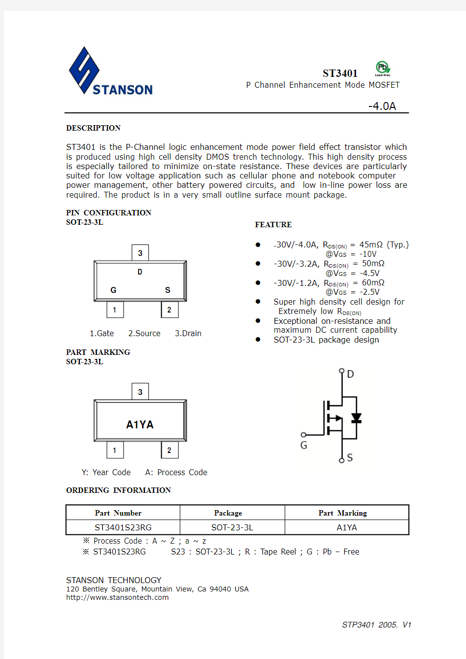
PIN CONFIGURATION SOT-23-3L FEATURE
z -30V/-4.0A, R DS(ON) = 45m Ω (Typ.)
@V GS = -10V
z -30V/-3.2A, R DS(ON) = 50m Ω
@V GS = -4.5V
1.Gate
2.Source
3.Drain
PART MARKING
SOT-23-3L
Y: Year Code A: Process Code
ORDERING INFORMATION
Part Number Package Part Marking
ST3401S23RG
SOT-23-3L
A1YA
※ Process Code : A ~ Z ; a ~ z
※ ST3401S23RG S23 : SOT-23-3L ; R : Tape Reel ; G : Pb – Free
z -30V/-1.2A, R DS(ON) = 60m Ω @V GS = -2.5V
z Super high density cell design for
Extremely low R DS(ON)
z Exceptional on-resistance and maximum DC current capability z SOT-23-3L package design
ST3401
P Channel Enhancement Mode MOSFET
-4.0A
STANSON TECHNOLOGY
120 Bentley Square, Mountain View, Ca 94040 USA
ABSOULTE MAXIMUM RATINGS (Ta = 25℃ Unless otherwise noted )
Parameter Symbol Typical Unit
Drain-Source Voltage V DSS -30 V Gate-Source Voltage
V GSS ±12 V Continuous Drain CurrentTJ=150℃) T A =25℃ T A =70℃
I D
-4.0 -3.2
A
Pulsed Drain Current
I DM -15 A Continuous Source Current (Diode Conduction) I S -1.0 A Power Dissipation
T A =25℃
T A =70℃ P D
1.25 0.8
W
Operation Junction Temperature T J 150 ℃ Storage Temperature Range
T STG -55/150 ℃ Thermal Resistance-Junction to Ambient
R θJA
120
℃/W
ST3401
P Channel Enhancement Mode MOSFET
-4.0A
STANSON TECHNOLOGY
120 Bentley Square, Mountain View, Ca 94040 USA
ELECTRICAL CHARACTERISTICS ( Ta = 25℃ Unless otherwise noted )
Parameter Symbol
Condition Min Typ Max Unit
Static
Drain-Source Breakdown Voltage
V (BR)DSS V GS =0V,I D =
-250uA -30
V
Gate Threshold Voltage V GS(th) V DS =V GS ,I D =-250uA -0.4 -1.0 V Gate Leakage Current I GSS V DS =0V,V GS =±12V
±100
nA
V DS =-24V,V GS =0V -1
Zero Gate Voltage Drain Current
I DSS V DS =-24V,V GS =0V T J =55℃ -10
uA On-State Drain Current I D(on) V DS ≦-5V,V GS =-4.5V
-10 A
Drain-source On-Resistance R DS(on) V GS =-10V,I D =-4.0A V GS =-4.5V,I D =-3.2A V GS =-2.5V,I D =-1.2A
45 50 60
m Ω
Forward Transconductance g fs V DS =-5V,I D =
-4.0V 10 S Diode Forward Voltage V SD
I S =-1.0A,V GS =
0V -0.8 -1.2 V
Dynamic
Total Gate Charge Q g 14 21 Gate-Source Charge Q gs 1.9
Gate-Drain Charge Q gd V DS =-15V
V GS =-10V I D ?-4.0A
3.7
nC
Input Capacitance C iss 540 Output Capacitance C oss 131 Reverse Transfer Capacitance C rss V DS =-15V V GS =0V F=1MH z 105
pF
10 15 Turn-On Time t d(on) tr 15 25 31 50 Turn-Off Time
t d(off) tf
V DS =-15V V GS =-15V I D =-1A R L =6Ω R G =-10Ω
20 30
nS
ST3401
P Channel Enhancement Mode MOSFET
-4.0A
STANSON TECHNOLOGY
120 Bentley Square, Mountain View, Ca 94040 USA TYPICAL CHARACTERICTICS (25℃ Unless noted)
ST3401
P Channel Enhancement Mode MOSFET
-4.0A
STANSON TECHNOLOGY
120 Bentley Square, Mountain View, Ca 94040 USA TYPICAL CHARACTERICTICS (25℃ Unless noted)
ST3401
P Channel Enhancement Mode MOSFET
-4.0A
STANSON TECHNOLOGY
120 Bentley Square, Mountain View, Ca 94040 USA SOT-23-3L PACKAGE OUTLINE