24AA256-EST中文资料
? 2007 Microchip Technology Inc.DS21930B-page 1
24AA00/24LC00/24C00 24AA01/24LC01B 24AA014/24LC01424C01C 24AA02/24LC02B 24C02C
24AA024/24LC024 24AA025/24LC02524AA04/24LC04B 24AA08/24LC08B 24AA16/24LC16B 24AA32A/24LC32A 24AA64/24LC64/24FC6424AA128/24LC128/24FC12824AA256/24LC256/24FC256 24AA512/24LC512/24FC512
Features:
?128-bit through 512 Kbit devices
?Single supply with operation down to 1.7V for 24AAXX devices
?Low-power CMOS technology:-
1mA active current, typical
-1μA standby current, typical (I-temp)
?2-wire serial interface bus, I 2C? compatible ?Schmitt Trigger inputs for noise suppression ?Output slope control to eliminate ground bounce ?100kHz (1.7V) and 400kHz (≥ 2.5V) compatibility ? 1 MHz for 24FCXX products
?Self-timed write cycle (including auto-erase)?Page write buffer
?Hardware write-protect available on most devices ?Factory programming (QTP) available ?ESD protection > 4,000V ? 1 million erase/write cycles ?Data retention > 200 years
?8-lead PDIP , SOIC, TSSOP and MSOP packages ?5-lead SOT-23 package (most 1-16 Kbit devices)?8-lead 2x3mm and 5x6mm DFN packages available
?Pb-free and RoHS compliant
?Available for extended temperature ranges:-Industrial (I): -40°C to +85°C -Automotive (E): -40°C to +125°C
Description:
The Microchip Technology Inc. 24CXX, 24LCXX,24AAXX and 24FCXX (24XX*) devices are a family of 128-bit through 512 Kbit Electrically Erased PROMs.The devices are organized in blocks of x8-bit memory with 2-wire serial interfaces. Low-voltage design permits operation down to 1.7V (for 24AAXX devices),with standby and active currents of only 1 μA and 1mA, respectively. Devices 1 Kbit and larger have page write capability. Parts having functional address lines allow connection of up to 8 devices on the same bus.The 24XX family is available in the standard 8-pin PDIP , surface mount SOIC, TSSOP and MSOP pack-ages. Most 128-bit through 16 Kbit devices are also available in the 5-lead SOT-23 package. DFN packages (2x3mm or 5x6mm) are also available. All packages are Pb-free (Matte Tin) finish.
*24XX is used in this document as a generic part number for 24 series devices in this data sheet.24XX64, for example, represents all voltages of the 64Kbit device.
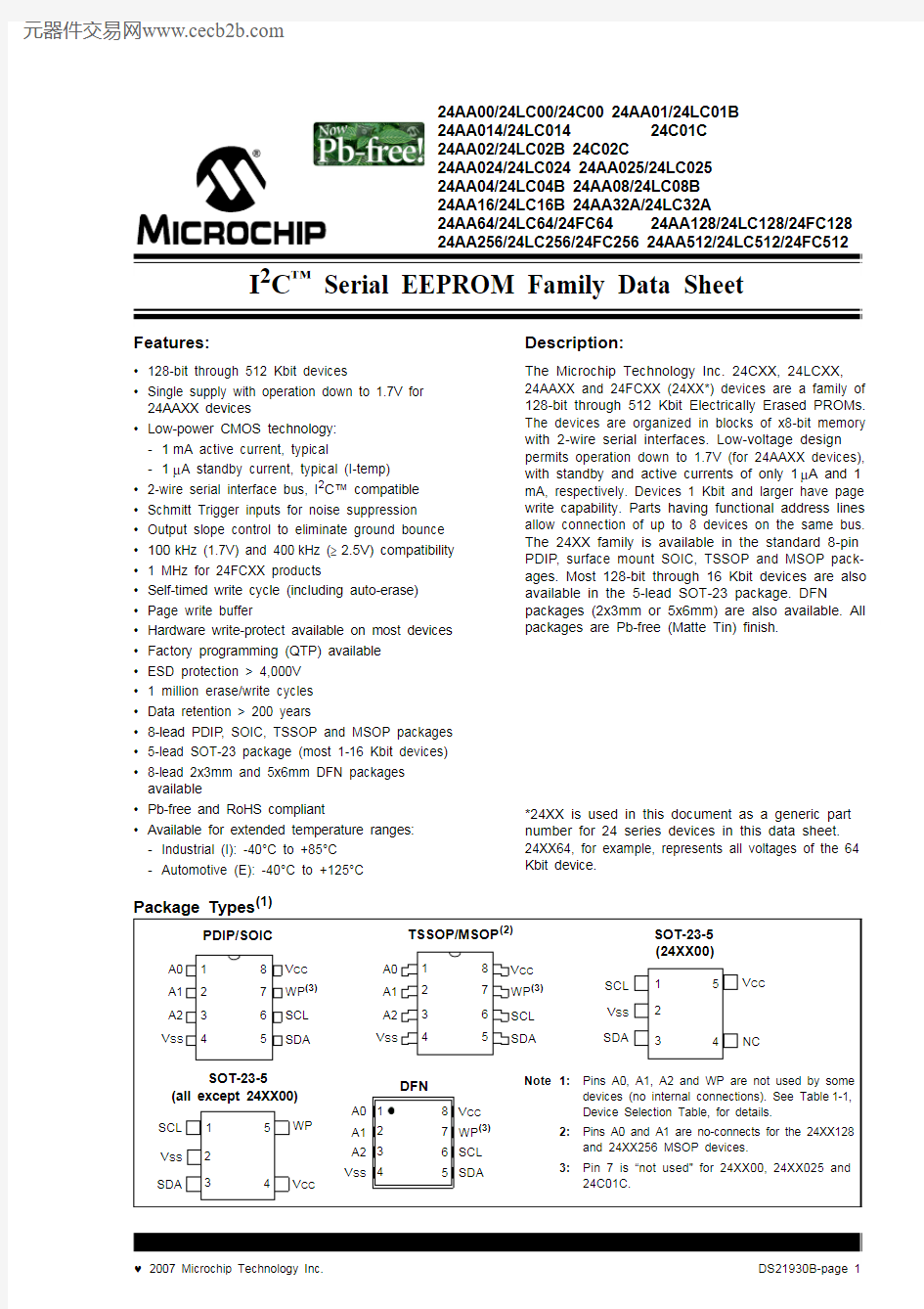
Package Types (1)
A0A1A2V SS
1234
8765
V CC WP (3)SCL SDA
PDIP/SOIC
A0A1A2V SS
1234
8765
V CC WP (3)SCL SDA TSSOP/MSOP (2)
15
4
3
SCL V SS SDA
V CC
NC 2SOT-23-5(24XX00)
SOT-23-5
15
4
3
SCL V SS SDA
WP
V CC 2(all except 24XX00)
A0A1A2V SS WP (3)SCL SDA
56784
321
V CC DFN
Note 1:
Pins A0, A1, A2 and WP are not used by some devices (no internal connections). See Table 1-1,Device Selection Table, for details.
2:
Pins A0 and A1 are no-connects for the 24XX128and 24XX256 MSOP devices.
3:Pin 7 is “not used” for 24XX00, 24XX025 and 24C01C.
I 2C ? Serial EEPROM Family Data Sheet
24AAXX/24LCXX/24FCXX
DS21930B-page 2? 2007 Microchip Technology Inc.
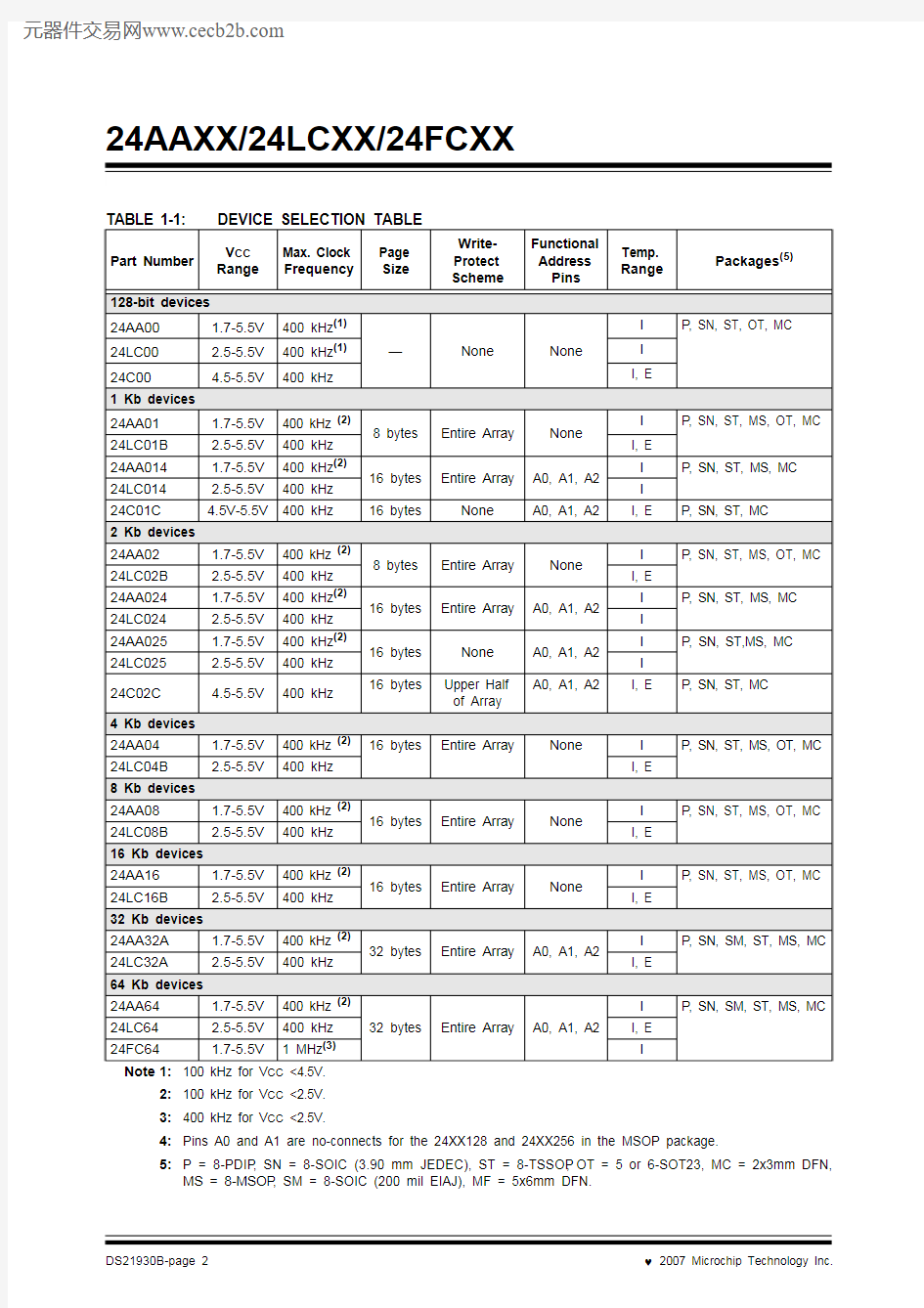
TABLE 1-1:
DEVICE SELECTION TABLE
Part Number V CC Range
Max. Clock Frequency
Page Size
Write-Protect Scheme
Functional Address Pins
Temp. Range
Packages (5)
128-bit devices 24AA00 1.7-5.5V 400 kHz (1)—
None
None
I P , SN, ST, OT, MC
24LC00 2.5-5.5V 400 kHz (1)I 24C00 4.5-5.5V
400 kHz
I, E
1 Kb devices 24AA01 1.7-5.5V 400 kHz (2)8 bytes Entire Array None I P , SN, ST, MS, OT, MC
24LC01B 2.5-5.5V 400 kHz I, E 24AA014 1.7-5.5V 400 kHz (2)16 bytes Entire Array A0, A1, A2I P , SN, ST, MS, MC 24LC014 2.5-5.5V
400 kHz
I 24C01C 4.5V-5.5V 400 kHz
16 bytes
None
A0, A1, A2
I, E
P , SN, ST, MC 2 Kb devices 24AA02 1.7-5.5V 400 kHz (2)8 bytes Entire Array None I P , SN, ST, MS, OT, MC
24LC02B 2.5-5.5V 400 kHz I, E 24AA024 1.7-5.5V 400 kHz (2)16 bytes Entire Array A0, A1, A2I P , SN, ST, MS, MC 24LC024 2.5-5.5V 400 kHz I 24AA025 1.7-5.5V 400 kHz (2)16 bytes None A0, A1, A2I P , SN, ST,MS, MC 24LC025 2.5-5.5V 400 kHz I 24C02C 4.5-5.5V
400 kHz
16 bytes
Upper Half of Array
A0, A1, A2
I, E
P , SN, ST, MC 4 Kb devices 24AA04 1.7-5.5V 400 kHz (2)16 bytes
Entire Array
None
I P , SN, ST, MS, OT, MC
24LC04B 2.5-5.5V
400 kHz
I, E
8 Kb devices 24AA08 1.7-5.5V 400 kHz (2)16 bytes
Entire Array
None
I P , SN, ST, MS, OT, MC
24LC08B 2.5-5.5V
400 kHz
I, E
16 Kb devices 24AA16 1.7-5.5V 400 kHz (2)16 bytes
Entire Array
None
I P , SN, ST, MS, OT, MC
24LC16B 2.5-5.5V
400 kHz
I, E
32 Kb devices 24AA32A 1.7-5.5V 400 kHz (2)32 bytes
Entire Array
A0, A1, A2
I P , SN, SM, ST, MS, MC
24LC32A 2.5-5.5V
400 kHz
I, E
64 Kb devices 24AA64 1.7-5.5V 400 kHz (2)32 bytes
Entire Array
A0, A1, A2
I P , SN, SM, ST, MS, MC
24LC64 2.5-5.5V 400 kHz I, E 24FC64
1.7-5.5V
1 MHz (3)
I
Note 1:100 kHz for V CC <4.5V.
2:100 kHz for V CC <2.5V.3:400 kHz for V CC <2.5V.
4:Pins A0 and A1 are no-connects for the 24XX128 and 24XX256 in the MSOP package.
5:P = 8-PDIP , SN = 8-SOIC (3.90 mm JEDEC), ST = 8-TSSOP , OT = 5 or 6-SOT23, MC = 2x3mm DFN,
MS = 8-MSOP , SM = 8-SOIC (200 mil EIAJ), MF = 5x6mm DFN.
? 2007 Microchip Technology Inc.DS21930B-page 3
24AAXX/24LCXX/24FCXX
128 Kb devices 24AA128 1.7-5.5V 400 kHz (2)64 bytes
Entire Array
A0, A1, A2(4)
I P , SN, SM, ST, MS, MF, ST14
24LC128 2.5-5.5V 400 kHz I, E 24FC128 1.7-5.5V
1 MHz (3)
I
256 Kb devices 24AA256 1.7-5.5V 400 kHz (2)64 bytes
Entire Array
A0, A1, A2(4)
I P , SN, SM, ST, MS, MF, ST14
24LC256 2.5-5.5V 400 kHz I, E 24FC256 1.7-5.5V
1 MHz (3)
I
512 Kb devices 24AA512 1.7-5.5V 400 kHz (2)128 bytes
Entire Array
A0, A1, A2
I
P , SM, MF, ST14
24LC512 2.5-5.5V
400 kHz
I, E 24FC512
1.7-5.5V (3) 1 MHz
I
TABLE 1-1:
DEVICE SELECTION TABLE (CONTINUED)
Part Number V CC Range
Max. Clock Frequency
Page Size
Write-Protect Scheme
Functional Address Pins
Temp. Range
Packages (5)
Note 1:100 kHz for V CC <4.5V.
2:100 kHz for V CC <2.5V.3:400 kHz for V CC <2.5V.
4:Pins A0 and A1 are no-connects for the 24XX128 and 24XX256 in the MSOP package.
5:P = 8-PDIP , SN = 8-SOIC (3.90 mm JEDEC), ST = 8-TSSOP , OT = 5 or 6-SOT23, MC = 2x3mm DFN,
MS = 8-MSOP , SM = 8-SOIC (200 mil EIAJ), MF = 5x6mm DFN.
24AAXX/24LCXX/24FCXX
DS21930B-page 4? 2007 Microchip Technology Inc.
2.0
ELECTRICAL CHARACTERISTICS
Absolute Maximum Ratings (?)
V CC .............................................................................................................................................................................6.5V All inputs and outputs w.r.t. V SS .........................................................................................................-0.6V to V CC +1.0V Storage temperature ...............................................................................................................................-65°C to +150°C Ambient temperature with power applied................................................................................................-40°C to +125°C ESD protection on all pins ......................................................................................................................................................≥4kV
TABLE 2-1:DC CHARACTERISTICS
? NOTICE: Stresses above those listed under “Absolute Maximum Ratings” may cause permanent damage to the device. This is a stress rating only and functional operation of the device at those or any other conditions above those indicated in the operational listings of this specification is not implied. Exposure to maximum rating conditions for extended periods may affect device reliability.
DC CHARACTERISTICS Electrical Characteristics:Industrial (I):V CC = +1.7V to 5.5V T A = -40°C to +85°C Automotive (E):V CC = +2.5V to 5.5V T A = -40°C to 125°C
Param.No.Sym.Characteristic
Min.Max.Units Conditions
D1—A0, A1, A2, SCL, SDA and WP pins:
————
D2V IH High-level input voltage 0.7 V CC
—V —
D3V IL Low-level input voltage
—
0.3 V CC 0.2 V CC
V V V CC ≥ 2.5V V CC < 2.5V D4V HYS Hysteresis of Schmitt Trigger inputs (SDA, SCL pins)0.05 V CC —V (Note 1)
D5V OL Low-level output voltage —0.40V I OL = 3.0mA @ V CC = 2.5V D6I LI Input leakage current —±1μA V IN = V SS or V CC D7I LO Output leakage current —±1μA V OUT = V SS or V CC D8C IN , C OUT
Pin capacitance (all inputs/outputs)
—10pF V CC = 5.0V (Note 1)
T A = 25°C, F CLK = 1MHz D9
I CC Read Operating current
—
4001
μA mA 24XX128, 256, 512: V CC = 5.5V, SCL = 400 kHz
All except 24XX128, 256, 512: V CC = 5.5V, SCL = 400 kHz I CC Write
—35mA mA V CC = 5.5V, All except 24XX512V CC = 5.5V, 24XX512D10
I CCS
Standby current
—
1
μA
T A = -40°C to +85°C
SCL = SDA = V CC = 5.5V A0, A1, A2, WP = V SS or V CC —5μA
T A = -40°C to 125°C
SCL = SDA = V CC = 5.5V A0, A1, A2, WP = V SS or V CC —50μA
24C01C and 24C02C only SCL = SDA = V CC = 5.5V A0, A1, A2, WP = V SS or V CC
Note 1:This parameter is periodically sampled and not 100% tested.
24AAXX/24LCXX/24FCXX TABLE 2-2:AC CHARACTERISTICS – ALL EXCEPT 24XX00, 24C01C
AND 24C02C
AC CHARACTERISTICS Electrical Characteristics:
Industrial (I):V CC = +1.7V to 5.5V T A = -40°C to +85°C Automotive (E):V CC = +2.5V to 5.5V T A = -40°C to 125°C
Param.
No.
Sym.Characteristic Min.Max.Units Conditions
1F CLK Clock frequency—
—
—
—
100
400
400
1000
kHz 1.7V ≤ V CC< 2.5V
2.5V ≤ V CC≤ 5.5V
1.7V ≤ V CC<
2.5V 24FCXXX
2.5V ≤ V CC≤ 5.5V 24FCXXX
2T HIGH Clock high time4000
600
600
500—
—
—
—
ns 1.7V ≤ V CC< 2.5V
2.5V ≤ V CC≤ 5.5V
1.7V ≤ V CC<
2.5V 24FCXXX
2.5V ≤ V CC≤ 5.5V 24FCXXX
3T LOW Clock low time4700
1300
1300
500—
—
—
—
ns 1.7V ≤ V CC< 2.5V
2.5V ≤ V CC≤ 5.5V
1.7V ≤ V CC<
2.5V 24FCXXX
2.5V ≤ V CC≤ 5.5V 24FCXXX
4T R SDA and SCL rise time
(Note1)—
—
—
1000
300
300
ns 1.7V ≤ V CC< 2.5V
2.5V ≤ V CC≤ 5.5V
1.7V ≤ V CC≤ 5.5V 24FCXXX
5T F SDA and SCL fall time
(Note1)—
—
300
100
ns All except 24FCXXX
1.7V ≤ V CC≤ 5.5V 24FCXXX
6T HD:STA Start condition hold time4000
600
600
250—
—
—
—
ns 1.7V ≤ V CC< 2.5V
2.5V ≤ V CC≤ 5.5V
1.7V ≤ V CC<
2.5V 24FCXXX
2.5V ≤ V CC≤ 5.5V 24FCXXX
7T SU:STA Start condition setup time4700
600
600
250—
—
—
—
ns 1.7V ≤ V CC< 2.5V
2.5V ≤ V CC≤ 5.5V
1.7V ≤ V CC<
2.5V 24FCXXX
2.5V ≤ V CC≤ 5.5V 24FCXXX
8T HD:DAT Data input hold time0—ns(Note2)
9T SU:DAT Data input setup time250
100
100—
—
—
ns 1.7V ≤ V CC< 2.5V
2.5V ≤ V CC≤ 5.5V
1.7V ≤ V CC≤ 5.5V 24FCXXX
10T SU:STO Stop condition setup time4000
600
600
250—
—
—
—
ns 1.7V ≤ V CC< 2.5V
2.5V ≤ V CC≤ 5.5V
1.7V ≤ V CC<
2.5V 24FCXXX
2.5V ≤ V CC≤ 5.5V 24FCXXX
11T SU:WP WP setup time4000
600
600—
—
—
ns 1.7V ≤ V CC< 2.5V
2.5V ≤ V CC≤ 5.5V
1.7V ≤ V CC≤ 5.5V 24FCXXX
12T HD:WP WP hold time4700
1300
1300—
—
—
ns 1.7V ≤ V CC< 2.5V
2.5V ≤ V CC≤ 5.5V
1.7V ≤ V CC≤ 5.5V 24FCXXX
Note1:Not 100% tested. C B = total capacitance of one bus line in pF.
2:As a transmitter, the device must provide an internal minimum delay time to bridge the undefined region (minimum 300ns) of the falling edge of SCL to avoid unintended generation of Start or Stop conditions.
3:This parameter is not tested but ensured by characterization. For endurance estimates in a specific application, please consult the Total Endurance? Model, which can be obtained from Microchip’s web site:
https://www.wendangku.net/doc/2713738522.html,.
4:24FCXXX denotes the 24FC64, 24FC128, 24FC256 and 24FC512 devices.
? 2007 Microchip Technology Inc.DS21930B-page 5
24AAXX/24LCXX/24FCXX
DS21930B-page 6? 2007 Microchip Technology Inc.
13
T AA
Output valid from clock (Note 2)
————3500900900400ns
1.7V ≤ V CC <
2.5V 2.5V ≤ V CC ≤ 5.5V
1.7V ≤ V CC <
2.5V 24FCXXX 2.5V ≤ V CC ≤ 5.5V 24FCXXX 14T BUF
Bus free time: Time the bus must be free before a new transmission can start 470013001300500————ns
1.7V ≤ V CC <
2.5V 2.5V ≤ V CC ≤ 5.5V
1.7V ≤ V CC <
2.5V 24FCXXX 2.5V ≤ V CC ≤ 5.5V 24FCXXX 15T OF Output fall time from V IH minimum to V IL maximum C B ≤ 100pF
10 + 0.1C B
250250ns
All except 24FCXXX (Note 1)24FCXXX (Note 1)
16T SP Input filter spike suppression (SDA and SCL pins)—50ns All except 24FCXXX (Note 1)
17T WC Write cycle time (byte or page)—5ms
18
—
Endurance
1,000,000
—
cycles 25°C (Note 3)
TABLE 2-2:
AC CHARACTERISTICS – ALL EXCEPT 24XX00, 24C01C AND 24C02C (CONTINUED)
AC CHARACTERISTICS Electrical Characteristics:Industrial (I):V CC = +1.7V to 5.5V T A = -40°C to +85°C Automotive (E):V CC = +2.5V to 5.5V T A = -40°C to 125°C
Param.No.Sym.Characteristic
Min.Max.Units Conditions
Note 1:Not 100% tested. C B = total capacitance of one bus line in pF.
2:As a transmitter, the device must provide an internal minimum delay time to bridge the undefined region (minimum 300ns) of the falling edge of SCL to avoid unintended generation of Start or Stop conditions.3:This parameter is not tested but ensured by characterization. For endurance estimates in a specific application, please consult the Total Endurance? Model, which can be obtained from Microchip’s web site:https://www.wendangku.net/doc/2713738522.html,.4:24FCXXX denotes the 24FC64, 24FC128, 24FC256 and 24FC512 devices.
24AAXX/24LCXX/24FCXX TABLE 2-3:AC CHARACTERISTICS – 24XX00, 24C01C AND 24C02C
All Parameters apply across all recommended operating ranges unless otherwise noted Industrial (I):T A = -40°C to +85°C, V CC = 1.7V to 5.5V Automotive (E):T A = -40°C to +125°C, V CC = 4.5V to 5.5V
Parameter Symbol Min.Max.Units Conditions
Clock frequency F CLK—
—
—100
100
400
kHz 4.5V ≤ Vcc ≤ 5.5V (E Temp range)
1.7V ≤ Vcc ≤ 4.5V
4.5V ≤ Vcc ≤
5.5V
Clock high time T HIGH4000
4000
600—
—
—
ns 4.5V ≤ Vcc ≤ 5.5V (E Temp range)
1.7V ≤ Vcc ≤ 4.5V
4.5V ≤ Vcc ≤
5.5V
Clock low time T LOW4700
4700
1300—
—
—
ns 4.5V ≤ Vcc ≤ 5.5V (E Temp range)
1.7V ≤ Vcc ≤ 4.5V
4.5V ≤ Vcc ≤
5.5V
SDA and SCL rise time (Note1)T R—
—
—
1000
1000
300
ns 4.5V ≤ Vcc ≤ 5.5V (E Temp range)
1.7V ≤ Vcc ≤ 4.5V
4.5V ≤ Vcc ≤
5.5V
SDA and SCL fall time T F—300ns(Note1)
Start condition hold time T HD:STA4000
4000
600—
—
—
ns 4.5V ≤ Vcc ≤ 5.5V (E Temp range)
1.7V ≤ Vcc ≤ 4.5V
4.5V ≤ Vcc ≤
5.5V
Start condition setup time T SU:STA4700
4700
600—
—
—
ns 4.5V ≤ Vcc ≤ 5.5V (E Temp range)
1.7V ≤ Vcc ≤ 4.5V
4.5V ≤ Vcc ≤
5.5V
Data input hold time T HD:DAT0—ns(Note2)
Data input setup time T SU:DAT250
250
100—
—
—
ns 4.5V ≤ Vcc ≤ 5.5V (E Temp range)
1.7V ≤ Vcc ≤ 4.5V
4.5V ≤ Vcc ≤
5.5V
Stop condition setup time T SU:STO4000
4000
600—
—
—
ns 4.5V ≤ Vcc ≤ 5.5V (E Temp range)
1.7V ≤ Vcc ≤ 4.5V
4.5V ≤ Vcc ≤
5.5V
Output valid from clock (Note2)T AA—
—
—
3500
3500
900
ns 4.5V ≤ Vcc ≤ 5.5V (E Temp range)
1.7V ≤ Vcc ≤ 4.5V
4.5V ≤ Vcc ≤
5.5V
Bus free time: Time the bus must be free before a new transmis-sion can start T BUF4700
4700
1300
—
—
—
ns 4.5V ≤ Vcc ≤ 5.5V (E Temp range)
1.7V ≤ Vcc ≤ 4.5V
4.5V ≤ Vcc ≤
5.5V
Output fall time from V IH minimum to V IL maximum T OF20+0.1
CB
250ns(Note1), CB ≤ 100 pF
Input filter spike suppression
(SDA and SCL pins)
T SP—50ns(Note1)
Write cycle time T WC—4
1.5ms24XX00
24C01C, 24C02C
Endurance1,000,000—cycles(Note3)
Note1:Not 100% tested. C B = total capacitance of one bus line in pF.
2:As a transmitter, the device must provide an internal minimum delay time to bridge the undefined region (minimum 300 ns) of the falling edge of SCL to avoid unintended generation of Start or Stop conditions.
3:This parameter is not tested but ensured by characterization. For endurance estimates in a specific application, please consult the Total Endurance? Model which can be obtained at https://www.wendangku.net/doc/2713738522.html,.
? 2007 Microchip Technology Inc.DS21930B-page 7
24AAXX/24LCXX/24FCXX
DS21930B-page 8? 2007 Microchip Technology Inc.
FIGURE 2-1:
BUS TIMING DATA
(unprotected)
(protected)SCL SDA IN
SDA OUT
WP 5
7
6
16
3
2
8913
D4
4
10
1112
14
24AAXX/24LCXX/24FCXX
3.0PIN DESCRIPTIONS
The descriptions of the pins are listed in Table3-1.
TABLE 3-1:PIN FUNCTION TABLE
3.1A0, A1, A2 Chip Address Inputs The A0, A1 and A2 pins are not used by the 24XX01 through 24XX16 devices.
The A0, A1 and A2 inputs are used by the 24C01C, 24C02C, 24XX014, 24XX024, 24XX025 and the 24XX32 through 24XX512 for multiple device opera-tions. The levels on these inputs are compared with the corresponding bits in the slave address. The chip is selected if the compare is true.
For the 24XX128 and 24XX256 in the MSOP package only, pins A0 and A1 are not connected.
Up to eight devices (two for the 24XX128 and 24XX256 MSOP package) may be connected to the same bus by using different Chip Select bit combinations.
In most applications, the chip address inputs A0, A1 and A2 are hard-wired to logic ‘0’ or logic ‘1’. For applications in which these pins are controlled by a microcontroller or other programmable device, the chip address pins must be driven to logic ‘0’ or logic ‘1’before normal device operation can proceed.
3.2Serial Data (SDA)
This is a bidirectional pin used to transfer addresses and data into and out of the device. It is an open drain terminal. Therefore, the SDA bus requires a pull-up resistor to V CC (typical 10kΩ for 100kHz, 2kΩ for 400kHz and1MHz).
For normal data transfer, SDA is allowed to change only during SCL low. Changes during SCL high are reserved for indicating the Start and Stop conditions.3.3Serial Clock (SCL)
This input is used to synchronize the data transfer to and from the device.
3.4Write-Protect (WP)
This pin must be connected to either V SS or V CC. If tied to V SS, write operations are enabled. If tied to V CC, write operations are inhibited but read operations are not affected. See Table1-1 for the write-protect scheme of each device.
3.5Power Supply (V CC)
A V CC threshold detect circuit is employed which disables the internal erase/write logic if V CC is below 1.5V at nominal conditions. For the 24C00, 24C01C and 24C02C devices, the erase/write logic is disabled below 3.8V at nominal conditions.
Pin Name
8-Pin
PDIP and
SOIC
8-Pin
TSSOP and
MSOP
5-Pin SOT-23
24XX00
5-Pin SOT-23
All except
24XX00
14-Pin
TSSOP
8-Pin
5x6 DFN and
2x3 DFN
Function
A011(1)——11User configurable Chip Select(3) A122(1)——22User configurable Chip Select(3) A233——63User configurable Chip Select(3) V SS442274Ground
SDA553385Serial Data
SCL661196Serial Clock
(NC)——4—3, 4, 5,
10, 11, 12
—Not Connected
WP7(2)7(2)—5137Write-Protect Input
V CC8854148Power Supply
Note1:Pins 1 and 2 are not connected for the 24XX128 and 24XX256 MSOP packages.
2:Pin 7 is not used for 24XX00, 24XX025 and 24C01C.
3:Pins A0, A1 and A2 are not used by some devices (no internal connections). See Table1-1 for details.
? 2007 Microchip Technology Inc.DS21930B-page 9
24AAXX/24LCXX/24FCXX
DS21930B-page 10? 2007 Microchip Technology Inc.
4.0
FUNCTIONAL DESCRIPTION
Each 24XX device supports a bidirectional, 2-wire bus and data transmission protocol. A device that sends data onto the bus is defined as a transmitter, while a device receiving data is defined as a receiver. The bus has to be controlled by a master device which gener-ates the Serial Clock (SCL), controls the bus access and generates the Start and Stop conditions, while the 24XX works as slave. Both master and slave can operate as transmitter or receiver, but the master device determines which mode is activated.
Block Diagram
HV Generator
EEPROM Array Page Latches*
YDEC
XDEC
Sense Amp.R/W Control
M emory C ontrol L ogic
I/O C ontrol L ogic I/O
A0*A1*A2*SDA
SCL
V CC V SS
WP*
* A0, A1, A2, WP and page latches are not used by some devices.
See Table 1-1, Device Selection Table, for details.
24AAXX/24LCXX/24FCXX
5.0BUS CHARACTERISTICS
The following bus protocol has been defined:
?Data transfer may be initiated only when the bus
is not busy.
?During data transfer, the data line must remain
stable whenever the clock line is high. Changes in
the data line while the clock line is high will be
interpreted as a Start or Stop condition.
Accordingly, the following bus conditions have been
defined (Figure5-1).
5.1Bus Not Busy (A)
Both data and clock lines remain high.
5.2Start Data Transfer (B)
A high-to-low transition of the SDA line while the clock
(SCL) is high determines a Start condition. All
commands must be preceded by a Start condition.
5.3Stop Data Transfer (C)
A low-to-high transition of the SDA line while the clock
(SCL) is high determines a Stop condition. All
operations must be ended with a Stop condition.
5.4Data Valid (D)
The state of the data line represents valid data when,
after a Start condition, the data line is stable for the
duration of the high period of the clock signal.
The data on the line must be changed during the low
period of the clock signal. There is one clock pulse per
bit of data.
Each data transfer is initiated with a Start condition and
terminated with a Stop condition. The number of data
bytes transferred between Start and Stop conditions is
determined by the master device.
? 2007 Microchip Technology Inc.DS21930B-page 11
24AAXX/24LCXX/24FCXX
DS21930B-page 12? 2007 Microchip Technology Inc.
5.5
Acknowledge
Each receiving device, when addressed, is obliged to generate an acknowledge after the reception of each byte. The master device must generate an extra clock pulse which is associated with this Acknowledge bit.The device that acknowledges has to pull down the SDA line during the acknowledge clock pulse in such a way that the SDA line is stable low during the high period of the acknowledge related clock pulse. Of course, setup and hold times must be taken into account. During reads, a master must signal an end-of-data to the slave by not generating an Acknowledge bit on the last byte that has been clocked out of the slave.In this case, the slave (24XX) will leave the data line high to enable the master to generate the Stop condition (Figure 5-2).
FIGURE 5-1:
DATA TRANSFER SEQUENCE ON THE SERIAL BUS
FIGURE 5-2:ACKNOWLEDGE TIMING
Note:
During a write cycle, the 24XX will not acknowledge commands.
SCL
SDA
(A)
(B)
(D)
(D)
(A)
(C)
Start Condition
Address or Acknowledge
Valid Data Allowed to Change
Stop Condition
SCL 987654321123
Transmitter must release the SDA line at this point,allowing the Receiver to pull the SDA line low to acknowledge the previous eight bits of data.
Receiver must release the SDA line at this point so the Transmitter can continue sending data.
Data from transmitter
SDA Acknowledge
bit
Data from transmitter
? 2007 Microchip Technology Inc.DS21930B-page 13
24AAXX/24LCXX/24FCXX
5.6
Device Addressing For Devices Without Functional Address Pins
A control byte is the first byte received following the Start condition from the master device (Figure 5-3).The control byte begins with a four-bit control code. For the 24XX, this is set as ‘1010’ binary for read and write operations. The next three bits of the control byte are the block-select bits (B2, B1, B0). They are used by the master device to select which of the 256-word blocks of memory are to be accessed. These bits are in effect the three Most Significant bits of the word address. Note that B2, B1 and B0 are “don’t care” for the 24XX00, the 24XX01 and 24XX02. B2 and B1 are “don’t care” for the 24XX04. B2 is “don’t care” for the 24XX08.
The last bit of the control byte defines the operation to be performed. When set to ‘1’, a read operation is selected. When set to ‘0’ a write operation is selected.Following the Start condition, the 24XX monitors the SDA bus. Upon receiving a ‘1010’ code, the block Acknowledge signal on the SDA line. The address byte follows the acknowledge.
FIGURE 5-3:
CONTROL AND ADDRESS BYTE ASSIGNMENTS FOR DEVICES WITHOUT ADDRESS PINS
S 1010x x x R/W ACK S 1010x x x R/W ACK S 1010x x x R/W ACK S 1010x x
B0
R/W ACK S 1010x
B1B0
R/W ACK S
1
1
B2B1B0
R/W
ACK
24XX0124XX0224XX0424XX0824XX016
x = “don’t care” bit
Acknowledge Control Code
Start bit
Control Byte
Block Select bits
Address Byte
24XX00Read/Write bit (read = 1, write = 0)
x x x x A3..A0x A6.....A0A7......A0A7......A0A7......A0A7
.
.
.
.
.
.
A0
bit
24AAXX/24LCXX/24FCXX
DS21930B-page 14? 2007 Microchip Technology Inc.
5.7
Device Addressing For Devices With Functional Address Pins
A control byte is the first byte received following the Start condition from the master device (Figure 5-4).The control byte begins with a 4-bit control code. For the 24XX, this is set as ‘1010’ binary for read and write operations. The next three bits of the control byte are the Chip Select bits (A2, A1, A0). The Chip Select bits allow the use of up to eight 24XX devices on the same bus and are used to select which device is accessed.The Chip Select bits in the control byte must corre-spond to the logic levels on the corresponding A2, A1and A0 pins for the device to respond. These bits are,in effect, the three Most Significant bits of the word address.
For 24XX128 and 24XX256 in the MSOP package, the A0 and A1 pins are not connected. During device addressing, the A0 and A1 Chip Select bits (Figure 5-4)should be set to ‘0’. Only two 24XX128 or 24XX256MSOP packages can be connected to the same bus.
The last bit of the control byte defines the operation to be performed. When set to a ‘1’, a read operation is selected. When set to a ‘0’, a write operation is selected.
For higher density devices (24XX32 through 24XX512), the next two bytes received define the address of the first data byte. Depending on the prod-uct density, not all bits in the address high byte are used. A15, A14, A13 and A12 are “don’t care” for 24XX32. A15, A14 and A13 are “don’t care” for 24XX64. A15 and A14 are “don’t care” for 24XX128.A15 is “don’t care” for 24XX256. All address bits are used for the 24XX512. The upper address bits are transferred first, followed by the Less Significant bits.Following the Start condition, the 24XX monitors the SDA bus. Upon receiving a ‘1010’ code, appropriate device select bits and the R/W bit, the slave device out-puts an Acknowledge signal on the SDA line. The address byte(s) follow the acknowledge.
FIGURE 5-4:
CONTROL AND ADDRESS BYTE ASSIGNMENTS FOR DEVICES WITH ADDRESS PINS
S 1010A2A1A0R/W ACK S 1010A2A1A0R/W ACK S 1010A2A1A0R/W ACK S 1010A2A1A0R/W ACK S
1
1
0A2A1A0R/W ACK
24XX6424XX12824XX25624XX512
x = “don’t care” bit
Acknowledge
Control Code Start bit
Control Byte
Chip Select bits*
Address High Byte
24XX32Read/Write bit
x x x x A11A10A9A8x x x
A12A11
A10A9A8x x
A13A12A11
A10A9A8x
A14A13A12A11
A10A9A8A15A14A13A12A11
A10
A9A8
bit
S 1010A2A1A0R/W ACK S 1010A2A1A0R/W ACK S
1
1
A2
A1
A0
R/W
ACK
x A6.....A0A7......A0A7
.
.
.
.
.
.
A0
24XX024/025
24C02C 24C01C Address Byte
A7......A0A7......A0A7......A0A7......A0A7
.
.
.
.
.
.
A0
Address Low Byte
* Chip Select bits A1 and A0 must be set to ‘0’ for 24XX128/256 devices in the MSOP package.
Control Byte
(Read = 1, Write = 0)
24AAXX/24LCXX/24FCXX 5.7.1CONTIGUOUS ADDRESSING
ACROSS MULTIPLE DEVICES
Chip Select bits A2, A1 and A0 can be used to expand
the contiguous address space by adding up to eight
24XXs on the same bus. Software can use the three
address bits of the control byte as the three Most
Significant bits of the address byte. For example, in the
24XX32 devices, software can use A0 of the control
byte as address bit A12; A1 as address bit A13; and A2
as address bit A14 (Table5-1). It is not possible to
sequentially read across device boundaries.
TABLE 5-1:CONTROL BYTE ADDRESS BITS
Maximum Devices
Maximum
Contiguous
Address Space
Chip Select Bit
A2
Chip Select Bit
A1
Chip Select Bit
A0
1K (24C01C)88 Kb A10A9A8
1K (24XX014)88 Kb A10A9A8
2K (24C02C)816 Kb A10A9A8
2K (24XX024/025)816 Kb A10A9A8
32K (24XX32)8256 Kb A14A13A12
64K (24XX64)8512 Kb A15A14A13
128K (24XX128)8* 1 Mb A16*A15*A14
256K (24XX256)8* 2 Mb A17*A16*A15
512K (24XX512)8 4 Mb A18A17A16
* Up to two 24XX128 or 24XX256 devices in the MSOP package can be added for up to 256 kb or 512 kb of address space, respectively. Bits A0 and A1 must be set to ‘0’.
? 2007 Microchip Technology Inc.DS21930B-page 15
24AAXX/24LCXX/24FCXX
DS21930B-page 16? 2007 Microchip Technology Inc.
6.0
WRITE OPERATIONS
6.1
Byte Write
A byte write operation begins with a Start condition from the master followed by the four-bit control code (see Figure 6-1 and Figure 6-2). The next 3 bits are either the Block Address bits (for devices without address pins) or the Chip Select bits (for devices with address pins). Then the master transmitter clocks the then generates an Acknowledge bit during the ninth clock cycle.
The next byte transmitted by the master is the address byte (for 128-bit to 16 Kbit devices) or the high-order address byte (for 32-512 Kbit devices). For 32 through 512 Kbit devices, the high-order address byte is followed by the low-order address byte. In either case,each address byte is acknowledged by the 24XX and the address bits are latched into the internal address counter of the 24XX.
For the 24XX00 devices, only the lower four address bits are used by the device. The upper four bits are “don’t cares.”
After receiving the ACK from the 24XX acknowledging the final address byte, the master device transmits the data word to be written into the addressed memory location. The 24XX acknowledges again and the master generates a Stop condition, which initiates the internal write cycle.
If an attempt is made to write to an array with the WP pin held high, the device will acknowledge the command, but no write cycle will occur, no data will be written, and the device will immediately accept a new command. After a byte Write command, the internal address counter will increment to the next address location. During a write cycle, the 24XX will not acknowledge commands.
FIGURE 6-1:
BYTE WRITE: 128-BIT TO 16 KBIT DEVICES
FIGURE 6-2:
BYTE WRITE: 32 TO 512 KBIT DEVICES
S
P
Bus Activity Master
SDA Line Bus Activity
S T A R T S T O P Control Byte
Address Byte
Data A C K
A C K
A C K
Byte
Bus Activity Master
SDA Line Bus Activity
S T A R T Control Byte
High Order Address Byte
Low Order Address Byte
Data S T O P A C K
A C K
A C K
A C K
S
P
Byte
? 2007 Microchip Technology Inc.DS21930B-page 17
24AAXX/24LCXX/24FCXX
6.2
Page Write
The write control byte, word address byte(s), and the first data byte are transmitted to the 24XX in much the same way as in a byte write (see Figure 6-3 and Figure 6-4). The exception is that instead of generating a Stop condition, the master transmits up to one page of bytes (1), which is temporarily stored in the on-chip page buffer. This data is then written into memory once the master has transmitted a Stop condition. Upon receipt of each word, the internal address counter is incremented by one. If the master should transmit more than one page of data prior to generating the Stop con-dition, the address counter will roll over and the previ-ously received data will be overwritten. As with the byte write operation, once the Stop condition is received, an internal write cycle begins. During the write cycle, the 24XX will not acknowledge commands.
Page writes can be any number of bytes within a page (up to the page size), starting at any address. Only the data bytes being addressed will be changed within the page.
If an attempt is made to write to the array with the WP pin held high, the device will acknowledge the command, but no write cycle will occur, no data will be written and the device will immediately accept a new command.
6.3
Write-Protection
The WP pin allows the user to write-protect the array when the pin is tied to V CC . See Device Selection Table 1-1 for the write-protect scheme of each device.If tied to V SS , the write protection is disabled. The WP pin is sampled prior to the Stop bit for every Write command (Figure 2-1). Toggling the WP pin after the Stop bit will have no effect on the execution of the write cycle.FIGURE 6-3:
PAGE WRITE: 1 KB TO 16 KBIT DEVICES
FIGURE 6-4:
PAGE WRITE: 32 TO 512 KBIT DEVICES
* See Table 1-1 for maximum number of data bytes in a page.
Note 1:See Device Selection Table 1-1 for the
page size of each device.
Note:
Page write operations are limited to writing bytes within a single physical page, regardless of the number of bytes actually being written. Physical page boundaries start at addresses that are integer multiples of the page buffer size (or ‘page size’) and end at addresses that are integer multiples of [page size – 1]. If a Page Write command attempts to write across a physical page boundary, the result is that the data wraps around to the beginning of the current page (over-writing data previously stored there),instead of being written to the next page, as might be expected. It is there-fore necessary for the application soft-ware to prevent page write operations that would attempt to cross a page boundary.
S
P
Bus Activity Master SDA Line Bus Activity
S T A R T Control Byte
Address Byte
Initial Final S T O P A C K
A C K
A C K
A C K
A C K
Second Data Byte
Data Byte
Data Byte*
Bus Activity Master SDA Line Bus Activity
S T A R T Control Byte
High Order Address Byte
Low Order Address Byte
Initial S T O P A C K
A C K
A C K
A C K
Final A C K
S
P
Data Byte
Data Byte*
24AAXX/24LCXX/24FCXX
DS21930B-page 18? 2007 Microchip Technology Inc.
7.0
ACKNOWLEDGE POLLING
Since the device will not acknowledge commands during a write cycle, this can be used to determine when the cycle is complete (This feature can be used to maximize bus throughput). Once the Stop condition for a Write command has been issued from the master,the device initiates the internally timed write cycle. ACK polling can be initiated immediately. This involves the master sending a Start condition, followed by the con-trol byte for a Write command (R/W = 0). If the device is still busy with the write cycle, then no ACK will be returned. If no ACK is returned, the Start bit and control byte must be re-sent. If the cycle is complete, then the device will return the ACK and the master can then pro-ceed with the next Read or Write command. See Figure 7-1 for flow diagram.
FIGURE 7-1:
ACKNOWLEDGE POLLING FLOW
Send
Write Command
Send Stop Condition to Initiate Write Cycle
Send Start
Send Control Byte with R/W = 0
Did Device Acknowledge (ACK = 0)?
Next Operation
No
Yes
? 2007 Microchip Technology Inc.DS21930B-page 19
24AAXX/24LCXX/24FCXX
8.0
READ OPERATION
Read operations are initiated in much the same way as the control byte is set to ‘1’. There are three basic types of read operations: current address read, random read and sequential read.
8.1Current Address Read
The 24XX contains an address counter that maintains the address of the last byte accessed, internally incre-mented by ‘1’. Therefore, if the previous read or write operation was to address ‘n ’ (n is any legal address),the next current address read operation would access data from address n + 1.
1’,the 24XX issues an acknowledge and transmits the 8-bit data byte. The master will not acknowledge the transfer, but does generate a Stop condition and the 24XX discontinues transmission (Figure 8-1).
FIGURE 8-1:
CURRENT ADDRESS READ
8.2
Random Read
Random read operations allow the master to access any memory location in a random manner. To perform this type of read operation, the byte address must first be set. This is done by sending the byte address to the 0’).Once the byte address is sent, the master generates a Start condition following the acknowledge. This termi-nates the write operation, but not before the internal address counter is set. The master then issues the control byte again, but with the R/W bit set to a ‘1’. The 24XX will then issue an acknowledge and transmit the 8-bit data byte. The master will not acknowledge the transfer but does generate a Stop condition, which causes the 24XX to discontinue transmission (Figure 8-2 and Figure 8-3). After a random Read command, the internal address counter will increment to the next address location.
FIGURE 8-2:
RANDOM READ: 128-BIT TO 16 KBIT DEVICES
FIGURE 8-3:
RANDOM READ: 32 TO 512 KBIT DEVICES
Bus Activity Master SDA Line Bus Activity
P
S
S T O P Control Byte
S T A R T Data A C K
N O A C K
Byte
S
P
S
Bus Activity Master
SDA Line Bus Activity
S T A R T S T O P Control Byte
A C K
Address Byte (n)
Control Byte
S T A R T Data A C K
A C K
N O A C K
Byte
Bus Activity Master
SDA Line Bus Activity
A C K
N O A C K
A C K
A C K
A C K
S T O P S T A R T Control Byte
High Order Address Byte
Low Order Address Byte
Control Byte
Data Byte
S T A R T S
S
P
24AAXX/24LCXX/24FCXX
DS21930B-page 20? 2007 Microchip Technology Inc.
8.3
Sequential Read
Sequential reads are initiated in the same way as a random read except that after the 24XX transmits the first data byte, the master issues an acknowledge as opposed to the Stop condition used in a random read.This acknowledge directs the 24XX to transmit the next sequentially addressed data byte (Figure 8-4). Follow-ing the final byte transmitted to the master, the master will NOT generate an acknowledge but will generate a Stop condition. To provide sequential reads, the 24XX contains an internal Address Pointer which is incre-mented by one at the completion of each operation.This Address Pointer allows the entire memory con-tents to be serially read during one operation. If the last address byte in the array is acknowledged, the Address Pointer will roll over to address 0x00.
FIGURE 8-4:
SEQUENTIAL READ
Bus Activity Master SDA Line Bus Activity
Control Byte
Data Byte
Data Byte
Data Byte
Data Byte
N O A C K
A C K
A C K
A C K
A C K
S T O P P
Initial Second Third Final