HCC4520BF中文资料

1/11
October 2002s
MEDIUM SPEED OPERATION :6MHz (Typ.) at 10V s POSITIVE -OR NEGATIVE- EDGE TRIGGERING s SYNCHRONOUS INTERNAL CARRY PROPAGATION
s QUIESCENT CURRENT SPECIF. UP TO 20V s 5V, 10V AND 15V PARAMETRIC RATINGS s INPUT LEAKAGE CURRENT
I I = 100nA (MAX) AT V DD = 18V T A = 25°C s 100% TESTED FOR QUIESCENT CURRENT s MEETS ALL REQUIREMENTS OF JEDEC JESD13B "STANDARD SPECIFICATIONS FOR DESCRIPTION OF B SERIES CMOS DEVICES"
DESCRIPTION
HCF4518B is a monolithic integrated circuit fabricated in Metal Oxide Semiconductor technology available in DIP and SOP packages. HCF4518B Dual BCD Up Counter consists of two identical, internal 4 stage counters. The counter stages are D-type Flip-Flops having interchangeable Clock and Enable lines for
incrementing on either the positive-going or negative going transitions. For single-unit operations the Enable input is maintained High and the counter advances on each positive going transition of the Clock. The counters are cleared by high levels on their Reset lines. The counter can be cascaded in the ripple mode by connecting Q4 to the enable input of the subsequent counter while the clock input of the latter is held low.
HCF4518B
DUAL BCD UP COUNTER
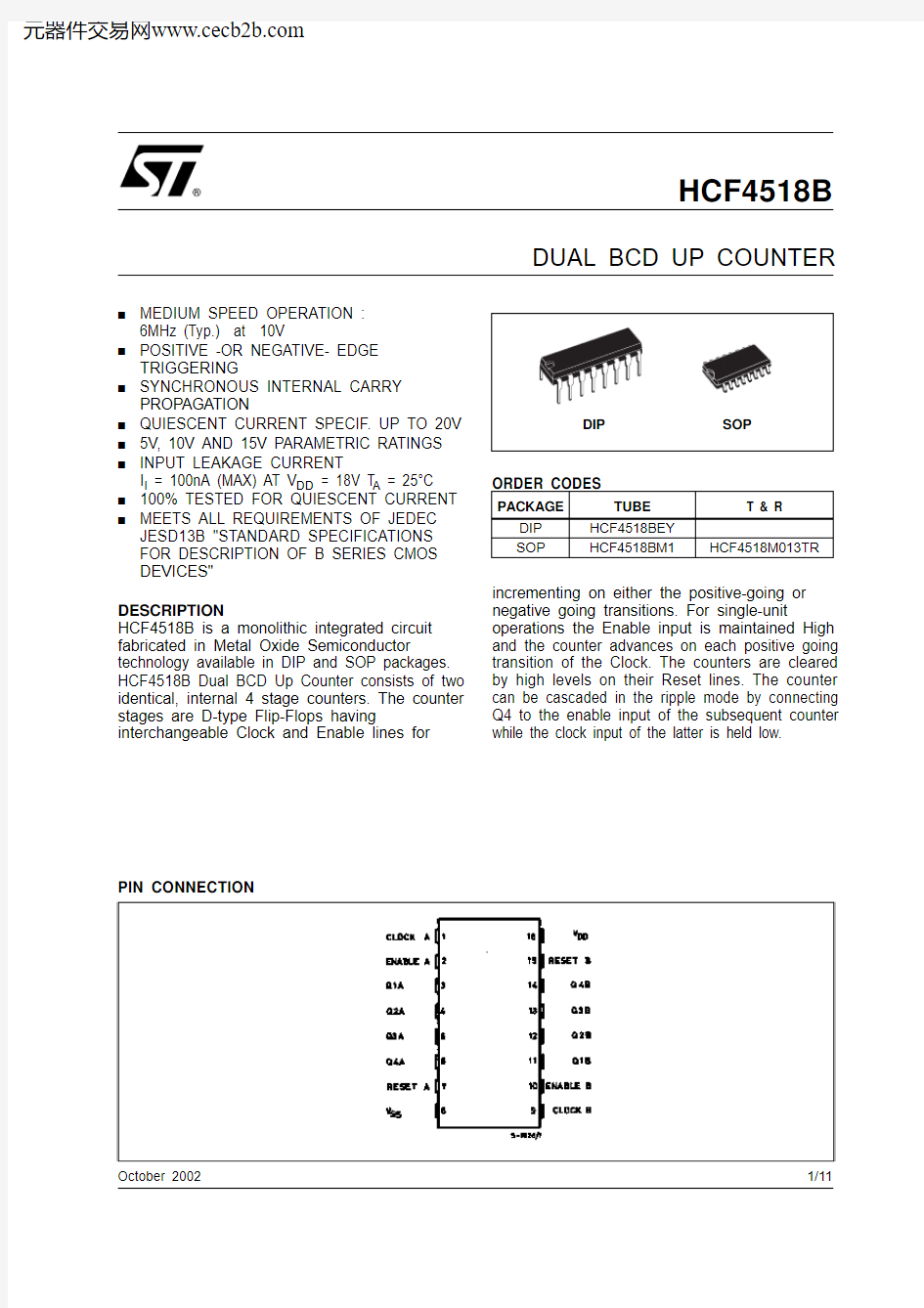
PIN CONNECTION
ORDER CODES
PACKAGE TUBE T & R DIP HCF4518BEY SOP
HCF4518BM1
HCF4518M013TR
HCF4518B
2/11
IINPUT EQUIVALENT CIRCUIT
PIN DESCRIPTION
FUNCTIONAL DIAGRAM
TRUTH TABLE
PIN No SYMBOL NAME AND FUNCTION 1CLOCK A Clock A input 2ENABLE A Enable A Input 7RESET A Reset A Input 3, 4, 5, 6
Q1A to Q4A Data Outputs 9CLOCK B Clock B input 10ENABLE B Enable B Input 15
RESET B Reset B Input 11,12,13,14
Q1B to Q4B
Data Outputs
8V SS
Negative Supply Voltage 16
V DD
Positive Supply Voltage
HCF4518B LOGIC DIAGRAM
TIMING CHART
3/11
HCF4518B
4/11
ABSOLUTE MAXIMUM RATINGS
Absolute Maximum Ratings are those values beyond which damage to the device may occur. Functional operation under these conditions is not implied.
All voltage values are referred to V SS pin voltage.
RECOMMENDED OPERATING CONDITIONS
Symbol Parameter
Value Unit V DD Supply Voltage -0.5 to +22V V I DC Input Voltage -0.5 to V DD + 0.5
V I I DC Input Current
± 10mA P D Power Dissipation per Package
200mW Power Dissipation per Output Transistor 100mW T op Operating Temperature -55 to +125°C T stg
Storage Temperature
-65 to +150
°C
Symbol Parameter
Value Unit V DD Supply Voltage 3 to 20V V I Input Voltage
0 to V DD V T op
Operating Temperature
-55 to 125
°C
HCF4518B
5/11
DC SPECIFICATIONS
The Noise Margin for both "1" and "0" level is: 1V min. with V DD =5V, 2V min. with V DD =10V, 2.5V min. with V DD =15V
Symbol
Parameter
Test Condition
Value Unit
V I (V)V O (V)
|I O |(μA)V DD (V)
T A = 25°C -40 to 85°C -55 to 125°C Min.
Typ.Max.Min.
Max.Min.
Max.I L
Quiescent Current
0/550.045150150μA
0/10100.0410*******/15150.04206006000/20200.08
100
3000
3000
V OH
High Level Output Voltage
0/5<15 4.95 4.95 4.95V
0/10<1109.959.959.950/15<11514.95
14.95
14.95
V OL
Low Level Output Voltage
5/0<150.050.050.05V
10/0<1100.050.050.0515/0
<1150.050.05
0.05
V IH
High Level Input Voltage 0.5/4.5<15 3.5 3.5 3.5V
1/9<1107771.5/13.5<11511
11
11
V IL
Low Level Input Voltage 4.5/0.5<15 1.5 1.5 1.5V
9/1<11033313.5/1.5<1154
4
4
I OH
Output Drive Current
0/5 2.5<15-1.36-3.2-1.1-1.1mA
0/5 4.6<15-0.44-1-0.36-0.360/109.5<110-1.1-2.6-0.9-0.90/1513.5<115-3.0-6.8-2.4-2.4I OL
Output Sink Current
0/50.4<150.4410.360.36mA
0/100.5<110 1.1 2.60.90.90/15 1.5<1
15 3.0
6.8 2.4 2.4
I I
Input Leakage Current
0/18
Any Input 18
±10-5±0.1±1±1μA C I
Input Capacitance
Any Input
5
7.5
pF
HCF4518B
6/11
DYNAMIC ELECTRICAL CHARACTERISTICS (T amb = 25°C, C L = 50pF, R L = 200K ?, t r = t f = 20 ns)
(*) Typical temperature coefficient for all V DD value is 0.3 %/°C.
Symbol
Parameter
Test Condition
Value (*)Unit
V DD (V)Min.
Typ.Max.t PLH t PHL Propagation Delay Time
Clock or Enable to Output 5280560ns 101152301580160t PLH t PHL Propagation Delay Time
Reset to Output 5330650ns
101302251590170t TLH t THL Transition Time
5100200ns
1050100154080
t W
Clock Pulse Width
5200100ns
1010050157035t W
Reset Pulse Width
5250125ns
1011055158040t W
Enable Pulse Width
5400200ns
1020010015140
70
t r , t f
Clock or Enable Rise and Fall Time 515μs
1015155
f MAX
Maximum Clock Frequency
5 1.53MHz
10361548
t r , t f
Clock Input Rise or Fall Time
515μs
10515
5
HCF4518B
7/11
TEST CIRCUIT
C L = 50pF or equivalent (includes jig and probe capacitance)R L = 200K ?
R T = Z OUT of pulse generator (typically 50?)
WAVEFORM 1 : MINIMUM PULSE WIDTH AND REMOVAL TIME
(f=1MHz; 50% duty cycle)
HCF4518B
WAVEFORM 2 : PROPAGATION DELAY TIME, MINIMUM PULSE WIDTH (f=1MHz; 50% duty cycle)
TYPICAL APPLICATION
RIPPLE CASCADING OF FOUR COUNTERS WITH POSITIVE-EDGE TRIGGERING
8/11
HCF4518B Information furnished is believed to be accurate and reliable. However, STMicroelectronics assumes no responsibility for the consequences of use of such information nor for any infringement of patents or other rights of third parties which may result from its use. No license is granted by implication or otherwise under any patent or patent rights of STMicroelectronics. Specifications mentioned in this publication are subject to change without notice. This publication supersedes and replaces all information previously supplied. STMicroelectronics products are not authorized for use as critical components in life support devices or systems without express written approval of STMicroelectronics.
? The ST logo is a registered trademark of STMicroelectronics
? 2002 STMicroelectronics - Printed in Italy - All Rights Reserved
STMicroelectronics GROUP OF COMPANIES
Australia - Brazil - Canada - China - Finland - France - Germany - Hong Kong - India - Israel - Italy - Japan - Malaysia - Malta - Morocco Singapore - Spain - Sweden - Switzerland - United Kingdom - United States.
? https://www.wendangku.net/doc/4c12943127.html,
11/11