CYT6119AKN中文资料

Description
The CYT6119 is an efficient linear voltage regulator. It has extra low dropout voltage. At light
loads the typical dropout voltage is 15mV, at full load the typical dropout voltage is 600mV. The output voltage accuracy is better than 2%.
The CYT6119 has low ground current at 65uA, so it can help prolong battery life. The CYT6119 is specially designed for hand-held, battery-powered devices.
Features
? Typical 175mV dropout voltage at 150mA.
? Low Ground current at 65uA. (Typ.)
? Guaranteed 400mA output over the full
operating temperature range. ? Extremely tight load and line regulation. ?
Low temperature coefficient. ?
Current and thermal limiting.
? No-load
stability. ? Standard SOT-89-3 package. Pin Configuration
1
2
3
SOT-89
Top view
Applications
? Active SCSI terminators.
? Post regulators for switching supplies. ? Battery chargers.
?
High-efficiency linear power supplies.
? Computer motherboard, display, graphic card
DC/DC converter, such as 5V to 3.3V, 3.3V to 2.8V or 3.3V to 2.5V.
Typical Application
Ordering Information
CYT6119 _ _ _
PIN (1=>3): 1. G: OUT/GND/IN
2. N: GND/IN/OUT
OUT = 3.3V
2. B: V OUT = 2.8V
3. C: V OUT = 2.5V
4. D: V OUT = 1.8V
5. E: V OUT = 1.5V
6. F: V OUT = 3.0V
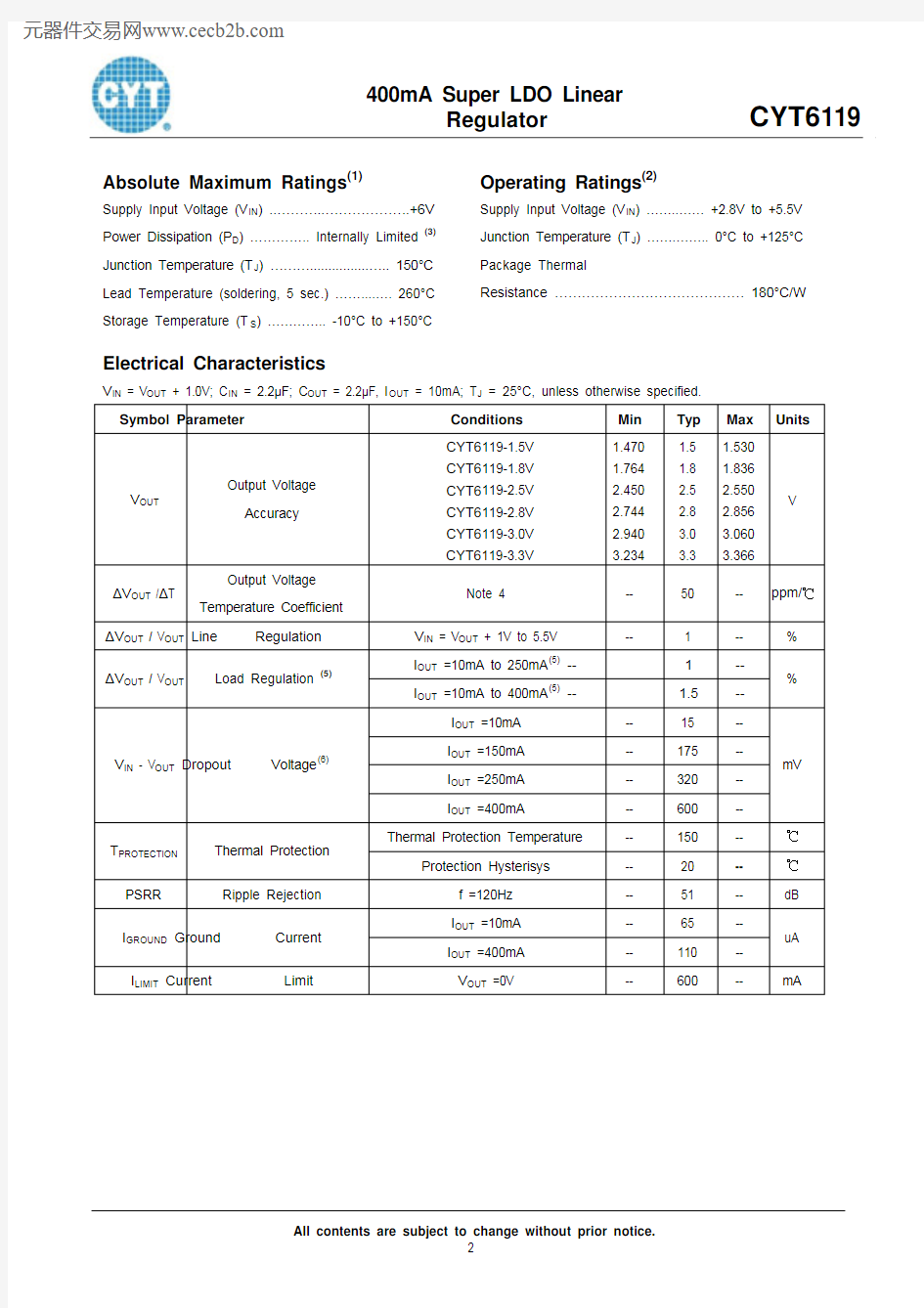
Absolute Maximum Ratings (1) Supply Input Voltage (V IN ) ..………..……………….+6V Power Dissipation (P D ) ………….. Internally Limited (3)
Junction Temperature (T J ) ………................….. 150°C Lead Temperature (soldering, 5 sec.) ……....…. 260°C Storage Temperature (T S ) ………….. -10°C to +150°C
Operating Ratings (2)
Supply Input Voltage (V IN ) ……..…… +2.8V to +5.5V Junction Temperature (T J ) …….…….. 0°C to +125°C Package Thermal
Resistance …………………………………… 180°C/W
Electrical Characteristics
V IN = V OUT + 1.0V; C IN = 2.2μF; C OUT = 2.2μF, I OUT = 10mA; T J = 25°C, unless otherwise specified. Symbol Parameter
Conditions Min Typ Max Units V OUT
Output Voltage Accuracy
CYT6119-1.5V CYT6119-1.8V
CYT6119-2.5V CYT6119-2.8V CYT6119-3.0V CYT6119-3.3V
1.470 1.764
2.450 2.744 2.940
3.234 1.5 1.8 2.5 2.8 3.0 3.3 1.530 1.836 2.550 2.856 3.060 3.366 V
?V OUT /?T
Output Voltage Temperature Coefficient
Note 4
-- 50 -- ppm/℃?V OUT / V OUT Line Regulation V IN = V OUT + 1V to 5.5V
--
1
--
% I OUT =10mA to 250mA (5) -- 1 --
?V OUT / V OUT
Load Regulation (5)
I OUT =10mA to 400mA (5) -- 1.5 --
%
I OUT =10mA
-- 15 -- I OUT =150mA -- 175 -- I OUT =250mA -- 320 -- V IN - V OUT Dropout Voltage (6)
I OUT =400mA
-- 600 -- mV
Thermal Protection Temperature
-- 150 -- ℃ T PROTECTION
Thermal Protection Protection Hysterisys
-- 20 -- ℃
PSRR
Ripple Rejection
f =120Hz -- 51 -- dB I OUT =10mA -- 65 -- I GROUND Ground Current I OUT =400mA -- 110 -- uA I LIMIT Current Limit V OUT =0V
--
600
--
mA
Note 1: Exceeding the absolute maximum rating may damage the device.
Note 2: The device is not guaranteed to function outside its operating rating.
Note 3: The maximum allowable power dissipation at any TA (ambient temperature) is calculated using: P D(MAX) = (T J(MAX) - T A)/θJA. Exceeding the maximum allowable power dissipation will result in excessive die temperature, and the regulator will go into thermal shutdown. See Table 1 and the “Thermal Considerations” section for details.
Note 4: Output voltage temperature coefficient is the worst-case voltage change divided by the total temperature range. Note 5: Regulation is measured at constant junction temperature using low duty cycle pulse testing. Parts are tested for load regulation in the load range from 100μA to 400mA. Changes in output voltage due to heating effects are covered by the thermal regulation specification.
Note 6: Dropout voltage is defined as the input to output differential at which the output voltage drops 2% below its nominal value measured at 1V differential.
Application Hints
Like any Low dropout regulator,CYT6119 requires external capacitors to ensure stability. The external capacitors must be carefully selected to ensure the performances.
Input Capacitor:
An Input Capacitor of at least 10uF is required. Ceramic or Tantalum can be used. The value can be increased without upper limit.
Output Capacitor:
An Output Capacitor is required for look stability. It must be located no more than 1cm away from the V OUT pin, and connected directly between V OUT and GND pins. The minimum value is 10uF but once again its value can be increased without limit. Thermal Consideration
It is important that the thermal limit of the package should not be exceeded. The CYT6119 has built-in thermal protection. When the thermal limit is exceeded, the IC will enter protection, and the V OUT will be reset to zero. The power dissipation for a given application can be calculated as follows:
The Power Dissipation (P D) is
P D = I OUT * [V IN – V OUT]
The thermal limit of the package is then limited to
P D(MAX) = [T J – T A]/θJA where T J is the junction temperature, T A is ambient temperature, and θJA is around 180°C/W for CYT6119. CYT6119 is designed to enter thermal protection at 150°C. For example, if T A is 25°C then the max P D is limited to about 0.7W. In other words, if I OUT(MAX) = 400mA, then [V IN –
V OUT] can not exceed 1.75V.
400mA Super LDO Linear
Regulator CYT6119
Line Transient Load Transient (10mA – 500mA)
400mA Super LDO Linear
Regulator
CYT6119
Outline Drawing for SOT-89