AK4566VN中文资料

ASAHI KASEI AKM CONFIDENTIAL [AK4566]
VCOM
SDTO
LRCK BICK
AINL1 AINL2
AINR1 AINR2
HPL
HPR
MOUT
LIN RIN MIN HVDD HVSS MUTET
AVDD AVSS SDTI
MCLK
CSN CCLK CDTI
PDN
DVDD
DVSS
VREF
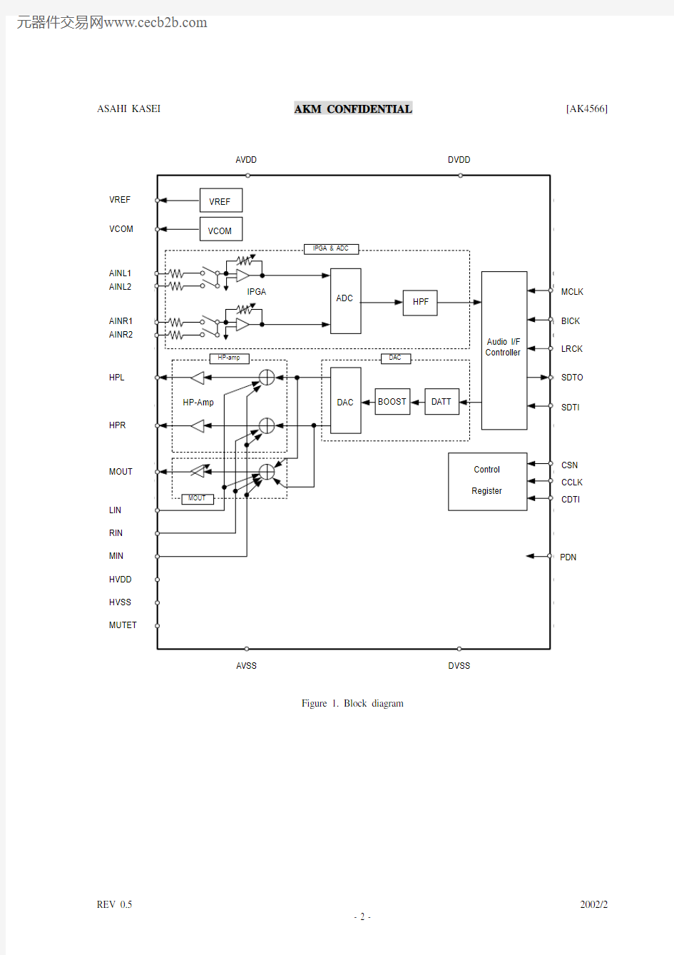
Figure 1. Block diagram
ASAHI KASEI AKM CONFIDENTIAL[AK4566] n Ordering Guide
AK4566VN -40 ~ +85°C 28pin QFN (0.5mm pitch)
AKD4566 Evaluation board for AK4566
n Pin Layout
PDN
A
I
N
L
1 1
CSN
2
8 2
CCLK 3 CDTI 4 LRCK 5 MCLK 6 BICK 7
A
I
N
R
1
2
7
A
I
N
L
2
2
6
2
5
2
4
A
V
S
S
2
3
V
C
O
M
2
2
S
D
T
I
8
S
D
T
O
9
D
V
D
D
1
D
V
S
S
1
1
H
V
S
S
1
2
1
3
H
P
R
1
4
21
20
19
18
17
16
15
VREF
LIN
RIN
MIN
MOUT
MUTET
HPL
Top View
H
V
D
D
A
I
N
R
2
A
V
D
D
ASAHI KASEI AKM CONFIDENTIAL[AK4566]
PIN/FUNCTION
No. Pin Name I/O Function
1 PDN I Power-down Pin
When at “L”, the AK4566 is in power-down mode and is held in reset. The AK4566 should always be reset upon power-up.
2 CSN I Control Data Chip Select Pin
3 CCLK I Control Clock Input Pin
4 CDTI I Control Data Input Pin
5 LRCK I L/R Clock Pin
This clock determines which audio channel is currently being output on SDTO pin and input on SDTI pin.
6 MCLK I Master Clock Input Pin
7 BICK I Serial Bit Clock Pin
This clock is used to latch audio data.
8 SDTI I Audio Data Input Pin
9 SDTO O Audio Data Output Pin
SDTO pin goes to DVSS when PDN pin is “L”.
10 DVDD - Digital Power Supply Pin
11 DVSS - Digital Ground Pin
12 HVSS - Ground Pin for Headphone Amplifier
13 HVDD - Power Supply Pin for Headphone Amplifier
14 HPR O Rch Headphone Amplifier Output Pin
HPR pin goes to HVSS when PDN pin is “L”.
15 HPL O Lch Headphone Amplifier Output Pin
HPL pin goes to HVSS when PDN pin is “L”.
16 MUTET O Mute Time Constant Control Pin
A capacitor for mute time constant should be connected between MUTET pin and HVSS
pin. MUTET pin goes to HVSS when PDN pin is “L”.
17 MOUT O Mono Analog Output Pin
MOUT pin goes to Hi-Z when PDN pin is “L”.
18 MIN I Mono Analog Input Pin
19 RIN I Rch Analog Input Pin
20 LIN I Lch Analog Input Pin
21 VREF O Reference Voltage Output Pin, 2.1V (typ, respect to AVSS)
Normally connected to AVSS pin with 0.1μF ceramic capacitor in parallel with a 4.7μF electrolytic capacitor. VREF pin goes to AVSS when PDN pin is “L”.
22 VCOM O Common Voltage Output Pin, 1.25V (typ, respect to AVSS)
Normally connected to AVSS pin with 0.1μF ceramic capacitor in parallel with a 2.2μF electrolytic capacitor. VCOM pin goes to AVSS when PDN pin is “L”.
23 AVSS - Analog Ground Pin
24 AVDD - Analog Power Supply Pin
25 AINR2 I Rch Analog Input 2 Pin for ADC (MIC Input)
26 AINL2 I Lch Analog Input 2 Pin for ADC (MIC Input)
27 AINR1 I Rch Analog Input 1 Pin for ADC (LINE Input)
28 AINL1 I Lch Analog Input 1 Pin for ADC (LINE Input) Note: No digital input pins must be left floating.
ASAHI KASEI AKM CONFIDENTIAL[AK4566]
ABSOLUATE MAXIMUM RATING
(AVSS, DVSS, HVSS=0V; Note 1)
Parameter Symbol min max Units
Power Supplies Analog
Digital
HP-AMP
|AVSS – HVSS| (Note 2)
|AVSS – DVSS| (Note 2) AVDD
DVDD
HVDD
?GND1
?GND2
-0.3
-0.3
-0.3
-
-
4.6
4.6
4.6
0.3
0.3
V
V
V
V
V
Input Current (any pins except for supplies) IIN - ±10 mA Analog Input Voltage (Note 3) VINA -0.3 (AVDD+0.3) or 4.6 V Digital Input Voltage (Note 4) VIND -0.3 (DVDD+0.3) or 4.6 V Ambient Temperature Ta -40 85 °C Storage Temperature Tstg -65 150 °C Note 1. All voltages with respect to ground.
Note 2. AVSS, DVSS and HVSS must be connected to the same analog ground plane.
Note 3. Max is smaller value between (AVDD+0.3) and 4.6V.
Note 4. Max is smaller value between (DVDD+0.3) and 4.6V.
WARNING: Operation at or beyond these limits may result in permanent damage to the device.
Normal operation is not guaranteed at these extremes.
RECOMMEND OPERATING CONDITIONS
(AVSS, DVSS, HVSS=0V; Note 1)
Parameter Symbol min typ max Units
Power Supplies Analog
Digital (Note 5)
HP-AMP AVDD
DVDD
HVDD
2.5
2.5 or (AVDD-0.3)
2.5
3.0
3.0
3.0
3.6
3.6 or (AVDD+0.3)
3.6
V
V
V
Note 1. All voltages with respect to ground.
Note 5. Min is larger value between 2.5V and (AVDD-0.3). Max is smaller value between 3.6V and (AVDD+0.3). * AKM assumes no responsibility for the usage beyond the conditions in this datasheet.
ASAHI KASEI AKM CONFIDENTIAL[AK4566]
ANALOG CHARACTERISTICS
(Ta=25°C; AVDD=DVDD=HVDD=3.0V, AVSS =DVSS=HVSS=0V; fs=44.1kHz; BOOST OFF; Signal Frequency
=1kHz; Measurement band width=20Hz ~ 20kHz; unless otherwise specified)
Parameter min Typ max Units ADC Resolution 20 bit IPGA Characteristics: (AINL1, AINR1 pins) (LINE IN)
Input Voltage 1.5 Vpp Input Resistance 25 50 k?Step Size 0.5 dB Gain Control Range -31 +20 dB IPGA Characteristics: (AINL2, AINR2 pins) (MIC IN)
Input Voltage 1.5 Vpp Input Resistance 6 12.5 k?Step Size 0.5 dB Gain Control Range -19 +32 dB ADC Characteristics: (Note 6)
S/(N+D) (-1dB Input) 82 dB D-Range (-60dB Input, A-weighted)) 88 dB S/N (A-weighted) 88 dB Interchannel Isolation 80 dB Interchannel Gain Mismatch 0.2 dB Power Supply Rejection (Note 11) 50 dB DAC Resolution 20 bit Headphone-Amp: (HPL/HPR pins) (Note 7) Load impedance is a serial connection with R L =22.8? and C L=100μF.
S/(N+D) (0dBFS Output) 50 dB D-Range (-60dBFS Output, A-weighted) 90 dB S/N (A-weighted) 90 dB Interchannel Isolation 80 dB Interchannel Gain Mismatch0.2 dB Load Resistance (Note 8) 20 ?
Load Capacitance (C1 in Figure 2)
(C2 in Figure 2) (Note 9) 30
300
pF
pF
Output Voltage 1.5 Vpp Power Supply Rejection (Note 11) 50 dB Mono Output: (MOUT pin) (Note 10)
S/(N+D) (0dBFS Output) 80 dB S/N (A-weighted) 88 dB Load Resistance (Note 8) 10 k?Load Capacitance 30 pF Output Voltage 1.5 Vpp Power Supply Rejection (Note 11) 50 dB Output Volume: (MOUT pin)
Step Size 2 dB Gain Control Range -30 0 dB Note 6. The signal inputs are AINL1/AINR1 or AINL2/AINR2. The value of IPGA is set to 0dB. On-chip HPF cancels the offset of IPGA and ADC.
Note 7. DACL=DACR= “1”, MINL=MINR=LIN=RIN= “0”, and ATTL=ATTR=0dB.
Note 8. AC Load
Note 9. The resistor larger than 6.8? is inserted in series.
Note 10. DACM= “1”, LINM=RINM=MINM= “0”, ATTL=ATTR=ATTM=0dB, and common mode signal is input to L/Rch of DAC.
Note 11. PSR is applied to AVDD, DVDD and HVDD with 1kHz, 50mVpp.
ASAHI KASEI AKM CONFIDENTIAL [AK4566]
Parameter min typ max Units
Analog Input: (LIN/RIN/MIN pins) Input Resistance 50 k ?
Gain LIN/RIN →MOUT
MIN →MOUT, LIN/MIN →HPL, RIN/MIN →HPR
-6 0 dB dB Power Supplies
Power Supply Current
Normal Operation (PDN= “H”)
AVDD + DVDD + HVDD (Note 12)
Power-Down Mode (PDN= “L”)
AVDD + DVDD + HVDD (Note 13) 16 10 mA μA
Note 12. All blocks are powered-up (PMVCM=PMADC=PMDAC=PMHPL=PMHPR=PMMO= “1”), and HP-Amp is no
output. 10mA (typ) at playback only (PMVCM=PMDAC=PMHPL=PMHPR=PMMO= “1”, PMADC= “0”).
Note 13. All digital input pins including clock pins (MCLK, BICK and LRCK) are held at DVDD or DVSS. PDN pin is
held at DVSS.
16?
Figure 2. Headphone amp output circuit
ASAHI KASEI AKM CONFIDENTIAL[AK4566]
FILTER CHARACTERISTICS
(Ta=25°C; AVDD, DVDD, HVDD=2.5 ~ 3.6V; fs=44.1kHz; DEM=OFF; BOOST=OFF)
Parameter Symbol min typ max Units ADC Digital Filter (LPF):
Passband (Note 15) ±0.1dB
-1.0dB
-3.0dB PB 0
-
-
20.0
21.1
17.4
-
-
kHz
kHz
kHz
Stopband (Note 15) SB 27.0 kHz Passband Ripple PR ±0.1 dB Stopband Attenuation SA 65 dB Group Delay (Note 16) GD - 17.0 - 1/fs Group Delay Distortion ?GD 0 μs ADC Digital Filter (HPF):
Frequency Response (Note 15) -3dB
-0.5dB
-0.1dB FR 3.4
10
22
Hz
Hz
Hz
DAC Digital Filter: (Note 14)
Passband (Note 15) ±0.01dB
?6.0dB PB 0
- 22.05
20.0
-
kHz
kHz
Stopband (Note 15) SB 24.1 kHz Passband Ripple PR ±0.06 dB Stopband Attenuation SA 43 dB Group Delay (Note 16) GD - 16.8 - 1/fs Group Delay Distortion ?GD 0 μs DAC Digital Filter + Analog Filter: (Note 14)(Note 17)
Frequency Response 0 ~ 20.0kHz FR - ±0.5 - dB BOOST Filter: (Note 17) (Note 18)
MIN 20Hz
100Hz
1kHz
FR -
-
-
5.74
2.92
-
-
-
dB
dB
dB
MID 20Hz
100Hz
1kHz
FR -
-
-
5.94
4.71
0.14
-
-
-
dB
dB
dB
Frequency Response
MAX 20Hz
100Hz
1kHz
FR -
-
-
16.04
10.55
0.3
-
-
-
dB
dB
dB
Note 14. BOOST OFF (BST1-0 = “00”)
Note 15. The passband and stopband frequencies scale with fs.
For example (DAC), PB=0.4535*fs(@±0.05dB), SB=0.546*fs(@-43dB).
Note 16. This is the calculated delay time caused by digital filtering. This time is measured from the input of analog signal to setting the 20 bit data of both channels on input register to the output register of ADC. This time also includes group delay of HPF. For DAC, this time is from setting the 20 bit data of both channels on input register to the output of analog signal.
Note 17. DACL à HPL, DACR à HPR, DACL/R à MOUT.
Note 18. These frequency responses scale with fs. If high-level signal is input, the AK4566 clips at low frequency.
ASAHI KASEI AKM CONFIDENTIAL[AK4566]
Figure 3. Boost Frequency (fs=44.1kHz)
DC CHARACTERISTICS
(Ta=25°C; AVDD, DVDD, HVDD = 2.5 ~ 3.6V)
Parameter Symbol min typ max Units
High-Level Input Voltage
Low-Level Input Voltage
Input Voltage at AC Coupling (Note 19)VIH
VIL
VAC
70%DVDD
-
1.0
-
30%DVDD
V
V
Vpp
High-Level Output Voltage (Iout = -100μA) Low-Level Output Voltage (Iout = 100μA)VOH
VOL
DVDD-0.4
-
-
-
-
0.4
V
V
Input Leakage Current Iin--±10μA Note 19. When AC coupled capacitor is connected to MCLK pin.
ASAHI KASEI AKM CONFIDENTIAL[AK4566]
SWITCHING CHARACTERISTICS
(Ta=25°C; AVDD, DVDD, HVDD = 2.5 ~ 3.6V: C L = 20pF)
Parameter Symbol min typ max Units Master Clock Timing
Frequency
Pulse Width Low (Note 20) Pulse Width High (Note 20) AC Pulse Width (Note 21)
fCLK
tCLKL
tCLKH
tACW
2.048
0.4/fCLK
0.4/fCLK
0.4/fCLK
24.576 MHz
ns
ns
ns
LRCK Timing
Frequency Duty Cycle
fs
Duty
8
45
44.1 48
55
kHz
%
Serial Interface Timing (Note 22)
BICK Period
BICK Pulse Width Low
Pulse Width High
LRCK Edge to BICK “↑” (Note 23) BICK “↑” to LRCK Edge (Note 23) LRCK to SDTO(MSB)
BICK “↓” to SDTO
SDTI Hold Time
SDTI Setup Time
tBCK
tBCKL
tBCKH
tLRB
tBLR
tLRS
tBSD
tSDH
tSDS
325.5
130
130
50
50
50
50
80
80
ns
ns
ns
ns
ns
ns
ns
ns
ns
Control Interface Timing
CCLK Period
CCLK Pulse Width Low
Pulse Width High CDTI Setup Time CDTI Hold Time
CSN “H” Time
CSN “↑” to CCLK “↑”CCLK “↑” to CSN “↑”
tCCK
tCCKL
tCCKH
tCDS
tCDH
tCSW
tCSS
tCSH
200
80
80
40
40
150
50
50
ns
ns
ns
ns
ns
ns
ns
ns
Power-down & Reset Timing
PDN Pulse Width (Note 24) PMADC “↑” to SDTO valid (Note 25)
tPD
tPDV
150
2081
ns
1/fs
Note 20. Except AC coupling.
Note 21. Pulse width to ground level when MCLK is connected to a capacitor in series and a resistor is connected to ground.
(Refer to Figure 4.)
Note 22. Refer to “Serial Data Interface”.
Note 23. BICK rising edge must not occur at the same time as LRCK edge.
Note 24. The AK4566 can be reset by bringing PDN= “L” to “H” only upon power up.
Note 25. This is the count of LRCK “↑” from PMADC bit=”1”.
ASAHI KASEI AKM CONFIDENTIAL [AK4566]
n Timing Diagram
MCLK Input
Measurement Point
AVSS
1000pF
VIH
MCLK
VIL
VIH LRCK
VIL
VIH BICK
VIL
Figure 5. Clock Timing
ASAHI KASEI AKM CONFIDENTIAL [AK4566]
LRCK
VIH BICK
VIL
SDTO
50%DVDD
VIH VIL
SDTI
VIH VIL
Figure 6. Serial Interface Timing
CSN
VIH CCLK
VIL
VIH CDTI
VIL
VIH
VIL
Figure 7. WRITE Command Input Timing
CSN
VIH CCLK
VIL
VIH CDTI VIL
VIH
VIL
D3D2D1D0
Figure 8. WRITE Data Input Timing
ASAHI KASEI AKM CONFIDENTIAL[AK4566]
CSN VIH VIL
SDTO
50%DVDD
PDN
VIL
Figure 9. Power-down & Reset Timing
ASAHI KASEI AKM CONFIDENTIAL[AK4566]
OPERATION OVERVIEW
n System Clock
The external clocks required to operate the AK4566 are MCLK(256fs/384fs/512fs), LRCK(fs) and BICK. The master clock (MCLK) should be synchronized with sampling clock (LRCK). The phase between these clocks does not matter. The frequency of MCLK is detected automatically, and the internal master clock becomes the appropriate frequency. Table 1 shows system clock example.
LRCK MCLK (MHz) BICK (MHz)
fs 256fs 384fs 512fs 64fs
8kHz 2.048 3.072 4.096 0.512
11.025kHz 2.8224 4.2336 5.6448 0.7056
12kHz 3.072 4.608 6.144 0.768
16kHz 4.096 6.144 8.192 1.024
22.05kHz 5.6448 8.4672 11.2896 1.4112
24kHz 6.144 9.216 12.288 1.536
32kHz 8.192 12.288 16.384 2.048
44.1kHz 11.2896 16.9344 22.5792 2.8224
48kHz 12.288 18.432 24.576 3.072
Table 1. System Clock Example
All external clocks (MCLK, BICK and LRCK) should always be present whenever the ADC or DAC is in normal operation mode (PMADC bit = “1” or PMDAC bit = “1”). If these clocks are not provided, the AK4566 may draw excess current and will not operate properly because it utilizes these clocks for internal dynamic refresh of registers. If the external clocks are not present, ADC and DAC should be placed in the power-down mode (PMADC bit = PMDAC bit = “0”). When MCLK is input with AC coupling, MCKAC bit should be set to “1”. When MCLK with AC coupling stops, MCKPD bit should be set to “1”.
When low sampling rate, DR and S/N degrade because of the outband noise. DR and S/N are approved by setting DFS bit to “1”. Table 2 shows S/N in the case DAC output to HP-amp and MOUT. When DFS bit is “1”, MCLK needs 512fs. When sampling frequency is changed at normal operation mode of ADC or DAC (PMADC bit = “1” or PMDAC bit = “1”), DAC output should be soft-muted or “0” data should be input to avoid click noise.
S/N (fs=8kHz, A-weighted)
DFS fs MCLK
HP-amp MOUT
0 8kHz~48kHz 256fs/384fs/512fs 84dB 84dB Default
1 8kHz~24kHz 512fs 90dB 88dB
Table 2. Relationship among fs, MCLK frequency and S/N of HP-amp and MOUT
ASAHI KASEI AKM CONFIDENTIAL [AK4566]
n Serial Data Interface
The AK4566 interfaces with external system by using BICK, LRCK, SDTO and SDTI pins. Four data formats are available and are selected by setting DIF1 and DIF0 bits (Table 3). Mode 0 of SDTI is compatible with existing 16bit DACs and digital filters. Mode 1 of SDTI is a 20bit version of Mode 0. Mode 2 of SDTI is similar to AKM ADCs and many DSP serial ports. Mode 3 is compatible with the I 2S serial data protocol. In Mode 2 and 3 of SDTI, 16bit data followed by four zeros also could be input, 18bit data followed by two zeros also could be input. In all modes, the serial data is MSB first and 2’s complement format.
Mode DIF1 DIF0 SDTO SDTI BICK LRCK 0 0 0 20bit, MSB justified 16bit, LSB justified ≥ 32fs H/L 1 0 1 20bit, MSB justified 20bit, LSB justified ≥ 40fs H/L 2 1 0 20bit, MSB justified 20bit, MSB justified ≥ 40fs
H/L Default 3 1 1 IIS (I 2S) IIS (I 2
S) 32fs or ≥ 40fs
L/H
Table 3. Audio Data Format
LRCK
BICK(64fs) SDTO(o)
SDTI(i)
BICK(32fs)
SDTI(i)
SDTO(o)
Figure 10. Mode 0 Timing
LRCK
BICK(64fs) SDTO(o) SDTI(i)
Figure 11. Mode 1 Timing
ASAHI KASEI AKM CONFIDENTIAL[AK4566]
LRCK
SDTO(o)
SDTI(i)
16bit
SDTI(i)
18bit
SDTI(i)
20bit
Figure 12. Mode 2 Timing Array
LRCK
SDTO(o)
SDTI(i)
16bit
SDTI(i)
18bit
SDTI(i)
20bit
SDTO(o)
SDTI(i)
Figure 13. Mode 3 Timing
n Digital High Pass Filter
The AK4566 has a Digital High Pass Filter (HPF) to cancel DC-offset in ADC and IPGA. The cut-off frequency of the HPF is 3.4Hz at fs=44.1kHz. It also scales with the sampling frequency (fs).
ASAHI KASEI AKM CONFIDENTIAL[AK4566] n ALC Operation
[1] ALC Limiter Operation
During the ALC limiter operation, when either output level of Lch or Rch in IPGA exceeds ALC limiter detection level set by LMTH bit, IPGA value is automatically attenuated by ALC limiter ATT step set by LMAT1-0 bits. Then the IPGA value is changed commonly for Lch and Rch.
At ZELMN bit = “1”, timeout period is set by LTM1-0 bits. The operation for attenuation is done continuously until the IPGA output signal level becomes LMTH or less. After finishing the operation for attenuation, unless ALC bit is changed to “0”, the operation of attenuation repeats when the IPGA output signal level exceeds LMTH.
At ZELMN bit = “0”, timeout period is set by ZTM1-0 bits. The IPGA value is automatically attenuated with zero crossing detection.
The ALC operation of the AK4566 corresponds to the impulse noise. If the impulse noise is supplied at ZELMN = “0”, the ALC limiter operation becomes the faster period than a set of ZTM1-0 bits. In case of ZELMN = “1”, it becomes the same period as LTM1-0 bits.
[2] ALC Recovery Operation
The ALC recovery operation waits until a time set by WTM1-0 bits after completing the ALC limiter operation. If the output signal does not exceed recovery waiting counter reset level set by LMTH bit, the ALC recovery operation is done. The IPGA value automatically increases by this operation up to the reference level set by REF6-0 bits with zero crossing detection which timeout period is set by ZTM1-0 bits. Then the IPGA value is set for Lch and Rch commonly. The ALC recovery operation is done at a period set by WTM1-0 bits. When zero cross is detected at the IPGA output during the wait period set by WTM1-0 bits, the ALC recovery operation waits until WTM1-0 period and the next recovery operation is done.
During the ALC recovery operation or the recovery waiting, when either output signal level of Lch or Rch in IPGA exceeds the ALC limiter detection level set by LMTH bit, the ALC recovery operation changes into the ALC limiter operation immediately.
In case of
(Recovery waiting counter reset level) ≤ (IPGA output level) < (Limiter detection level)
during the ALC recovery operation, the waiting timer of ALC recovery operation is reset. Therefore, when (Recovery waiting counter reset level) > (IPGA output level),
the waiting timer of ALC recovery operation starts.
The ALC operation of the AK4566 corresponds to the impulse noise. If the impulse noise is supplied, the ALC recovery operation becomes the faster period than a set of ZTM1-0 or WTM1-0 bits.
Others:
When either channel enters the limiter operation during the waiting time of zero crossing, the present ALC recovery operation stops, according as the small value of IPGA (a channel waiting zero crossing), the ALC limiter operation is done. When both channels are waiting for the next ALC recovery operation, the ALC limiter operation is done from the IPGA value of a point in time.
ZTM1-0 bits set zero crossing timeout and WTM1-0 bits set the ALC recovery operation period. When the ALC recovery waiting time (WTM1-0 bits) is shorter than zero crossing timeout period (ZTM1-0 bits), the ALC recovery is operated by the zero crossing timeout period. Therefore, in this case, the ALC recovery operation period is not constant.
ASAHI KASEI AKM CONFIDENTIAL[AK4566] [3] ALC Operation Example
The following registers should not be changed during the ALC operation:
LTM1-0, LMTH, LMAT1-0, WTM1-0, ZTM1-0, RATT, REF6-0, ZELMN.
Figure 14. Registers set-up sequence at ALC operation (WR=Write)
ASAHI KASEI AKM CONFIDENTIAL[AK4566] n IPGA Operation
[Write Operation at ALC Enabled]
The values of IPGA6-0 bits are ignored during ALC operation.
[Write Operation at ALC Disabled]
Channel independent zero crossing detection is used. If there is no zero crossings, then the level will change after a timeout. The ZTM1-0 bits set the zero crossing timeout. When the IPGA7-0 bits are written by μP, the zero crossing counter is reset and starts. When the IPGA output signal detects zero crossing or zero crossing timeout, the written value by μP becomes valid.
When writing to the IPGA7-0 bits continually, the control register should be written by an interval more than zero crossing timeout. If not, there is a possibility that each IPGA of L/R channels has a different gain. [IPGA Gain after completing ALC operation]
The IPGA7-0 bits are not updated by the actual gain of IPGA changed during ALC operation. In order to set the actual gain of IPGA with the IPGA7-0 bits, the IPGA7-0 bits should be written after zero crossing timeout period when completing ALC operation (ALC bit= “1” à “0”).
ASAHI KASEI AKM CONFIDENTIAL[AK4566] n Digital Attenuator
The AK4566 has channel-independent digital attenuator (256 levels, 0.5dB step). This digital attenuator is placed before D/A converter. ATTL/R7-0 bits set the attenuation level (0dB to -127dB or MUTE) of each channel (Table 19). At DATTC= “1”, ATTL7-0 bits control both Lch and Rch attenuation level. At DATTC= “0”, ATTL7-0 bits control Lch level and ATTR7-0 bits control Rch level.
ATS bit set the transition time between set values of ATT7-0 bits as either 1061/fs or 7424/fs (Table 15). At ATS= “0”, the transition between set values is soft transition of 1062 levels. It takes 1061/fs (24ms@fs=44.1kHz) from FFH(0dB) to 00H(MUTE). The ATTs are 00H when PMDAC bit is “0”. When PMDAC returns to “1”, the ATTs fade to their current value. Digital attenuator is independent of soft mute function.
n Soft Mute
Soft mute operation is performed in the digital domain. When SMUTE bit goes to “1”, the output signal is attenuated by -∞(“0”) via the cycle set by TM1-0 bit (Table 18). When SMUTE bit returns to “0”, the mute is cancelled and the output attenuation gradually changes to 0dB via the cycle set by TM1-0 bits. If the soft mute is cancelled within the cycle set by TM1-0 bits after starting the operation, the attenuation is discontinued and returned to 0dB. The soft mute is effective for changing the signal source without stopping the signal transmission.
Attenuation
-
Analog Output
Figure 15. Soft Mute Function
NOTE:
(1) The output signal is attenuated until -∞ (“0”) by the cycle set by TM1-0 bits.
(2) Analog output corresponding to digital input have the group delay (GD).
(3) If the soft mute is cancelled within the cycle set by TM1-0 bits, the attenuation is discontinued and returned to
0dB(the setting value).