SSM6J50TU中文资料

TOSHIBA Field Effect Transistor Silicon P Channel MOS Type (U-MOS Ⅲ)
SSM6J50TU
○ High Current Switching Applications
? Compact package suitable for high-density mounting
? Low on-resistance: R on = 205m ? (max) (@V GS = -2.0 V) R on = 100m ? (max) (@V GS = -2.5 V) R on = 64m ? (max) (@V GS = -4.5 V)
Absolute Maximum Ratings (Ta = 25°C)
Characteristics Symbol Rating Unit
Drain-Source voltage V DS -20 V Gate-Source voltage V GSS
±10 V DC I D -2.5 Drain current
Pulse I
DP
-5
A
Drain power dissipation P D
(Note 1)
500 mW Channel temperature T ch 150 °C Storage temperature range
T stg
?55~150
°C
Note: Using continuously under heavy loads (e.g. the application of
high temperature/current/voltage and the significant change in
temperature, etc.) may cause this product to decrease in the reliability significantly even if the operating conditions (i.e.
operating temperature/current/voltage, etc.) are within the absolute maximum ratings.
Please design the appropriate reliability upon reviewing the Toshiba Semiconductor Reliability Handbook (“Handling Precautions”/“Derating Concept and Methods”) and individual reliability data (i.e. reliability test report and estimated failure rate, etc). Note 1: Mounted on FR4 board.
(25.4 mm × 25.4 mm × 1.6 t, Cu Pad: 645 mm 2
)
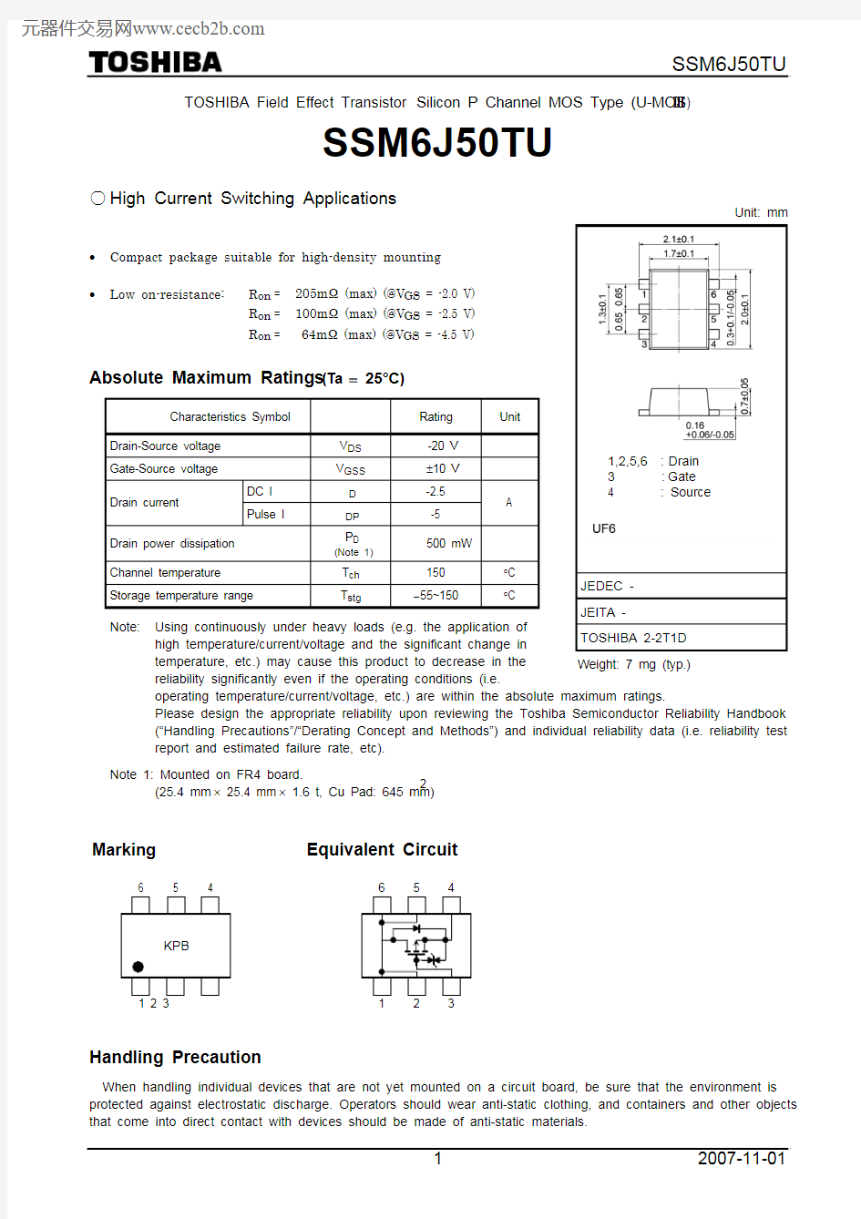
Marking Equivalent Circuit
Handling Precaution
When handling individual devices that are not yet mounted on a circuit board, be sure that the environment is
protected against electrostatic discharge. Operators should wear anti-static clothing, and containers and other objects that come into direct contact with devices should be made of anti-static materials.
Unit: mm
1,2,5,6 : Drain
3 : Gate
4 : Source
JEDEC - JEITA -
TOSHIBA 2-2T1D Weight: 7 mg (typ.)
Electrical Characteristics (Ta = 25°C)
Characteristics Symbol Test Condition Min Typ. Max Unit
Gate leakage current
I GSS V GS = ±8 V, V DS = 0 ? ? ±10μA V (BR) DSS I D = ?10 mA, V GS = 0 -20 ? ? Drain-Source breakdown voltage
V (BR) DSX
I D = ?10 mA, V GS = +10 V -10 ? ? V Drain cut-off current I DSS V DS = ?20 V, V GS = 0 ? ? ?10μ
A Gate threshold voltage V th V DS = ?10 V, I D = ?0.2 mA ?0.5 ? ?1.2
V
Forward transfer admittance
?Y fs ?
V DS = ?10 V, I D = ?1.5 A (Note2) 3.1
6.2
? S
I D = ?1.5 A, V GS = ?4.5 V
(Note2)? 49 64
I D = ?1.5 A, V GS = ?2.5 V (Note2)?
73 100m Ω
Drain-Source on-resistance
R DS (ON)
I D = ?1.5 A, V GS = ?2.0 V
(Note2)
?
105 205
Input capacitance
C iss V DS = ?10 V, V GS = 0, f = 1 MHz ? 800 ? pF
Reverse transfer capacitance C rss V DS = ?10 V, V GS = 0, f = 1 MHz ?
120
?
pF
Output capacitance C oss V DS = ?10 V, V GS = 0, f = 1 MHz ? 160 ? pF Turn-on time t on ? 15 ? Switching time
Turn-off time
t off
V DD = ?10 V, I D = ?1.5 A, V GS = 0~?5 V, R G = 4.7 Ω
?
51
?
ns
Note2: Pulse test
Switching Time Test Circuit
(a) Test Circuit
(b) V IN
Precaution
V th can be expressed as the voltage between gate and source when the low operating current value is I D =-200 μA for this product. For normal switching operation, V GS (on) requires a higher voltage than V th and V GS (off) requires a lower voltage than V th.
(The relationship can be established as follows: V GS (off) < V th < V GS (on)) Be sure to take this into consideration when using the device.
(c) V OUT
V DD = -10 V R G = 4.7 Ω D.U.< = 1%
V IN : t r , t f < 5 ns Common Source Ta = 25°C
0?5 V
10 μs I
0 V
?5 V V DS (ON)
V DD
Drain current ID (A)
D r a i n -S o u r c e o n -r e s i s t a n c e R D S (O N ) (m?)
Gate-Source voltage VGS(V)
R DS(ON)-Ta
D r a i n -S o u r c e o n -r e s i s t a n c e R D S (O N ) (m?)
Ambient temperature Ta(°C)
040
80
120
160
-80
-40
40
80
120
160
Vth-Ta
G a t e t h r e s h o l d v o l t a g e V t h (V )
Ambient temperature Ta(°C)
-2
-1.6
-1.2
-0.8
-0.4
0-80
-40
40
80
120
160
Drain current ID (A)
F o r w a r d t r a n s f e r a d m i t t a n c e
|Y f s |(S )
|Yfs|-I
D
0.11
10
100
-0.1
-0.3-1-3-10
C-V DS
C a p a c i t a n c e C (p F )
Drain-Source voltage V DS
(V)
10100
1000
10000
-0.1
-0.3-1-3-10-30-100
I DR -V DS
D r a i n r e v e r s e c u r r e n t I D R (A )
Drain-Source voltage V DS
(V)
0.2
0.40.60.81
-10
-3.0
-1.0
-0.3
- 0.1
Pulse width t w (s)
r th – t w
T r a n s i e n t t h e r m a l i m p e d a n c e r t h (°C /W )
0.001
1000
0.01 0.1 1
100
10 Drain-Source voltage V DS (V)
Safe operating area
D r a i n c u r r e n t I D (A )
D r a i n p o w e r d i s s i p a t
i o n P D (W )
Ambient temperature Ta (°C)
P D – Ta
RESTRICTIONS ON PRODUCT USE
20070701-EN GENERAL ?The information contained herein is subject to change without notice.
?TOSHIBA is continually working to improve the quality and reliability of its products. Nevertheless, semiconductor devices in general can malfunction or fail due to their inherent electrical sensitivity and vulnerability to physical stress. It is the responsibility of the buyer, when utilizing TOSHIBA products, to comply with the standards of safety in making a safe design for the entire system, and to avoid situations in which a malfunction or failure of such TOSHIBA products could cause loss of human life, bodily injury or damage to property.
In developing your designs, please ensure that TOSHIBA products are used within specified operating ranges as set forth in the most recent TOSHIBA products specifications. Also, please keep in mind the precautions and conditions set forth in the “Handling Guide for Semiconductor Devices,” or “TOSHIBA Semiconductor Reliability Handbook” etc.
? The TOSHIBA products listed in this document are intended for usage in general electronics applications (computer, personal equipment, office equipment, measuring equipment, industrial robotics, domestic appliances, etc.).These TOSHIBA products are neither intended nor warranted for usage in equipment that requires extraordinarily high quality and/or reliability or a malfunction or failure of which may cause loss of human life or bodily injury (“Unintended Usage”). Unintended Usage include atomic energy control instruments, airplane or spaceship instruments, transportation instruments, traffic signal instruments, combustion control instruments, medical instruments, all types of safety devices, etc.. Unintended Usage of TOSHIBA products listed in his document shall be made at the customer’s own risk.
?The products described in this document shall not be used or embedded to any downstream products of which manufacture, use and/or sale are prohibited under any applicable laws and regulations.
? The information contained herein is presented only as a guide for the applications of our products. No responsibility is assumed by TOSHIBA for any infringements of patents or other rights of the third parties which may result from its use. No license is granted by implication or otherwise under any patents or other rights of TOSHIBA or the third parties.
? Please contact your sales representative for product-by-product details in this document regarding RoHS compatibility. Please use these products in this document in compliance with all applicable laws and regulations that regulate the inclusion or use of controlled substances. Toshiba assumes no liability for damage or losses occurring as a result of noncompliance with applicable laws and regulations.