OB2532A Preliminary Datasheet_sz_110318

OB2532A
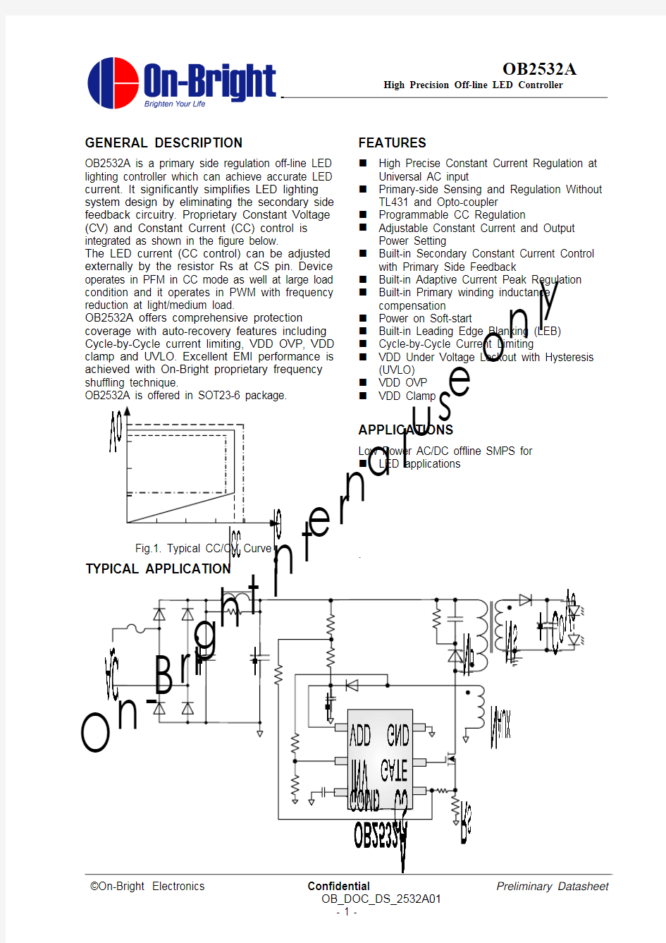
High Precision Off-line LED Controller
n
B
Ordering Information Part Number OB2532AMP SOT23-6, Pb-free, T&R
n -
r
i g h
t n t
e r
n
o
e
s
u
l
a
n
r
e
t
h
g
i
r
Figure.1 Auxiliary voltage waveform
is inversely proportional to the primary winding inductance changes. Up to variation of the primary winding inductance can be The output LED current is
s
oc th R _ Where N is the ratio of transformer between
primary side winding and secondary winding. Adjustable CC point and Output Power In OB2532A, the CC point and maximum output current sense resistor Rs at CS pin as illustrated in Typical Application Diagram. adjusted through CC point change. The larger Rs, the smaller CC point is, and the smaller output power becomes, and vice versa as shown in Fig.3.
u s e
o l
For flyback operating in DCM, The maximum output power is given by
2
max 21pk SW P O I F L P η= (4) Where Lp indicate the inductance of primary winding and Ip is the peak current of primary winding. Refer to the equation 3, the change of the primary winding inductance results in the change of the maximum output power and the constant output current in CC mode. To compensate the change from variations of primary winding inductance, the switching frequency is locked by an internal loop such that the switching frequency is Demag
SW T F 21= (4) Since T Demag is inversely proportional to the inductance, as a result, the product Lp and fsw is constant, thus the maximum output power and constant current in CC mode will not change as primary winding inductance changes. Up to +/-7% variation of the primary winding inductance can be compensated. z Frequency shuffling for EMI improvement The frequency shuffling (switching frequency modulation) is implemented in OB2532A. The oscillation frequency is modulated so that the tone energy is spread out. The spread spectrum minimizes the conduction band EMI and therefore eases the system design.
z
Current Sensing and Leading Edge Blanking
Cycle-by-Cycle current limiting is offered in OB2532A. The switch current is detected by a
sense resistor into the CS pin. An internal leading
edge blanking circuit chops off the sensed voltage spike at initial power MOSFET on state so that the external RC filtering on sense input is no longer needed. The PWM duty cycle is determined by the current sense input voltage and the EA output voltage. z Gate Drive The external power MOSFET is driven by a dedicated gate driver of OB2532A. Too weak the gate drive strength results in higher conduction
and switch loss of MOSFET while too strong gate
drive compromises EMI. A good tradeoff is achieved through the built-in
totem pole gate design with right output strength control. z Protection Control Good power supply system reliability is achieved with its rich protection features including Cycle-by-Cycle current limiting (OCP), VDD clamp, Power on Soft Start, and Under Voltage Lockout on VDD (UVLO).
VDD is supplied by transformer auxiliary winding
output. The output of OB2532A is shut down when VDD drops below UVLO (ON) limit and the power converter enters power on start-up sequence thereafter. O
n -
B r
i g h
t i
n t
e r n a l u s e
o n l y
IMPORTANT NOTICE
RIGHT TO MAKE CHANGES
On-Bright Electronics Corp. reserves the right to make corrections, modifications, enhancements, improvements and other changes to its products and services at any time and to discontinue any product or service without notice. Customers should obtain the latest relevant information before placing orders and should verify that such information is current and complete.
WARRANTY INFORMATION
On-Bright Electronics Corp. warrants performance of its hardware products to the specifications applicable at the time of sale in accordance with its standard warranty. Testing and other quality control techniques are used to the extent it deems necessary to support this warranty. Except where mandated by government requirements, testing of all parameters of each product is not necessarily performed.
On-Bright Electronics Corp. assumes no liability for application assistance or customer product design. Customers are responsible for their products and applications using On-Bright’s components, data sheet and application notes. To minimize the risks associated with customer products and applications, customers should provide adequate design and operating safeguards.
LIFE SUPPORT
On-Bright Electronics Corp.’s products are not designed to be used as components in devices intended to support or sustain human life. On-bright Electronics Corp. will not be held liable for any damages or claims resulting from the use of its products in medical applications.
MILITARY
On-Bright Electronics Corp.’s products are not designed for use in military applications. On-Bright Electronics Corp. will not be held liable for any damages or claims resulting from the use of its products in military applications.
O
n -
B r
i g h
t i
n t
e r n a l u s e
o n l y